

Normally-off compound semiconductor tunnel transistor
- Summary
- Abstract
- Description
- Claims
- Application Information
AI Technical Summary
Benefits of technology
Problems solved by technology
Method used
Image

Examples
Embodiment Construction
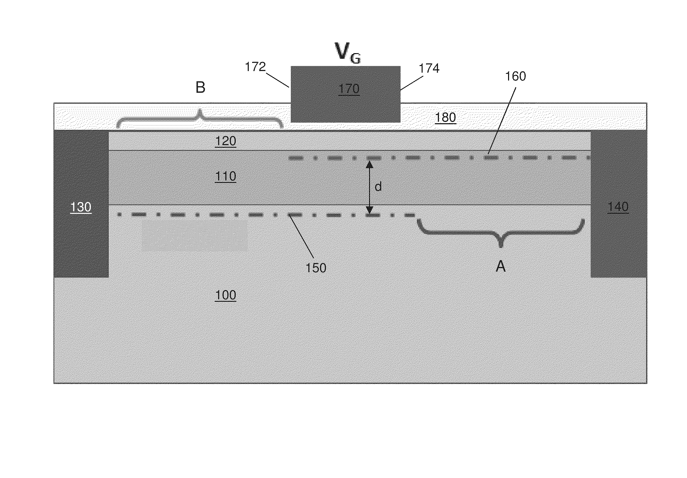
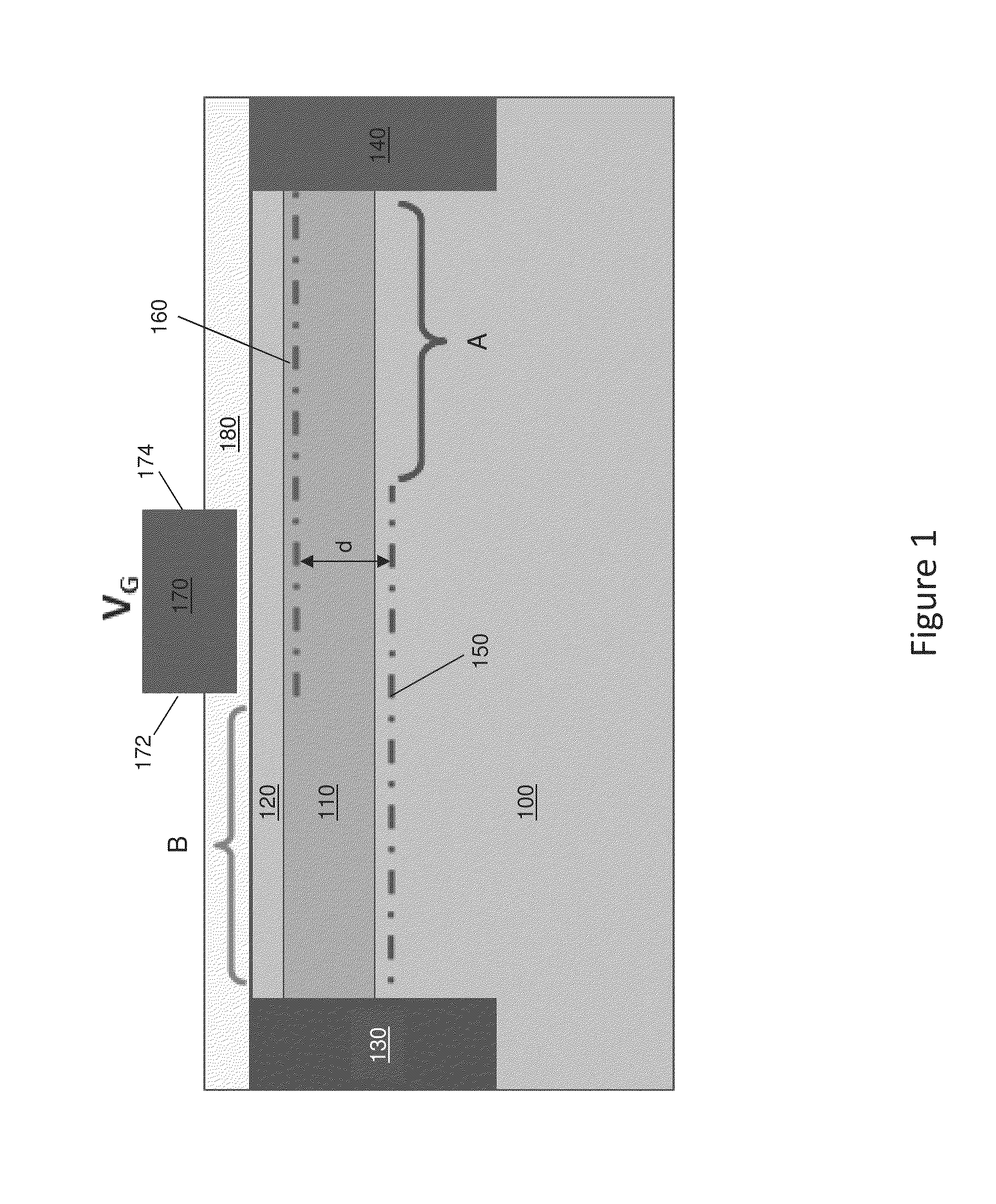
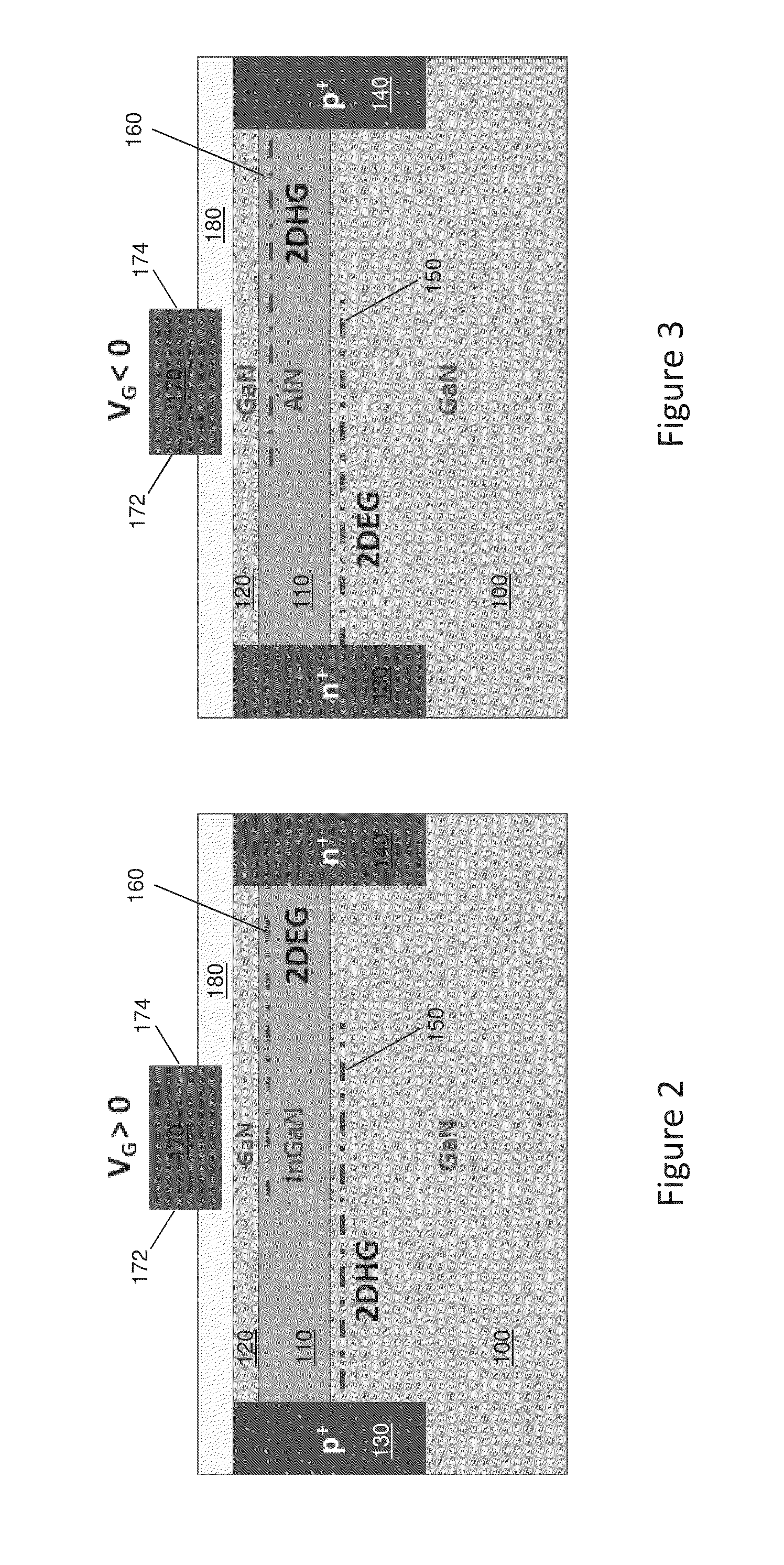
[0025]Described next are embodiments of a normally-off compound semiconductor tunnel field effect transistor having a relatively high drive current e.g. above 100 mA per mm of gate length and a relatively low sub-threshold slope e.g. below 60 mV per decade at room temperature, and methods of manufacturing such a normally-off compound semiconductor tunnel transistor. The compound semiconductor tunnel field effect transistor is fast-switching and can be used for high voltage applications e.g. 30V up to 600V and higher. The normally-off compound semiconductor tunnel transistor can be implemented in e.g. GaN technology. With GaN technology, the presence of polarization charges and strain effects result in the realization of a so-called “two-dimensional charge carrier gas” (also referred to herein as inversion layer) which is a two-dimensional electron or hole inversion layer characterized by very high carrier density and carrier mobility. The presence of such a two-dimensional charge ca...
PUM
 Abstract
Description
Claims
Application Information