Multi-voltage level semiconductor device and its manufacture

Inactive Publication Date: 2006-04-04
YAMAHA CORP
View PDF27 Cites 0 Cited by
  • Summary
  • Abstract
  • Description
  • Claims
  • Application Information

AI Technical Summary

Benefits of technology

[0015]It is possible to create a depletion layer in the gate electrode in high-voltage circuit MOS transistors on the channel side by reducing the doping of the impurity in the gate electrodes. By creating a depletion layer, the electric field applied to the gate oxide film in high-voltage circuit is decreased and hence the breakdown voltage is increased. Furthermore, by forming the gate oxide film more thickly at the edges thereof than in the central portion thereof, it is possible to increase the breakdown voltage in the edge regions of

Problems solved by technology

This increases the number of manufacturing steps, and hence causes manufacturing costs to increase.
A suitable thickness for high-voltage circuit gate oxide films will be unnecessarily thick for low-voltage circuits, and hence MOS transistor perfo

Method used


Image

  • Multi-voltage level semiconductor device and its manufacture
  • Multi-voltage level semiconductor device and its manufacture
  • Multi-voltage level semiconductor device and its manufacture

Examples


Example

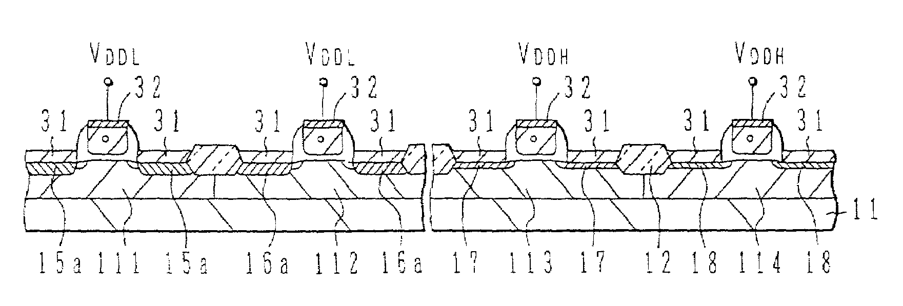
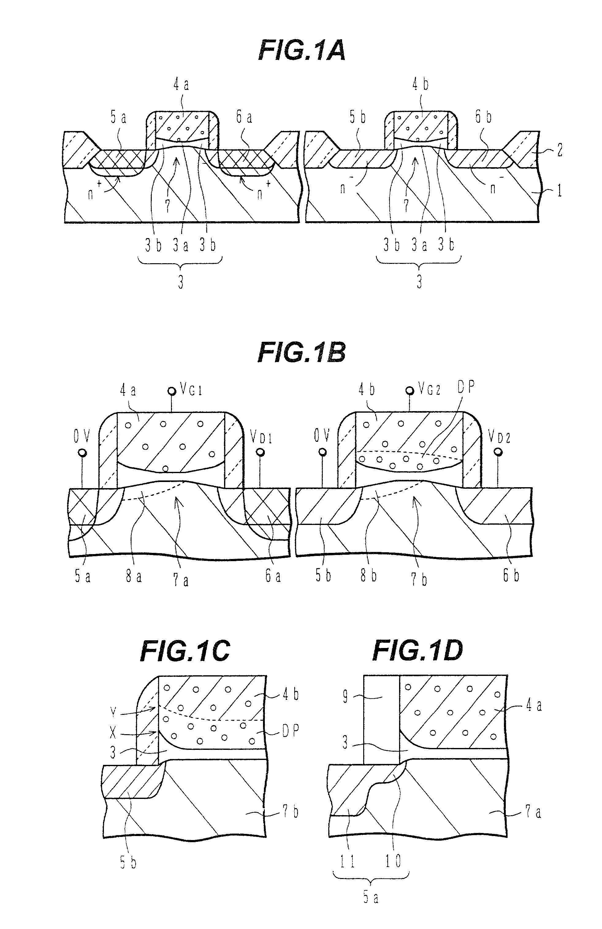
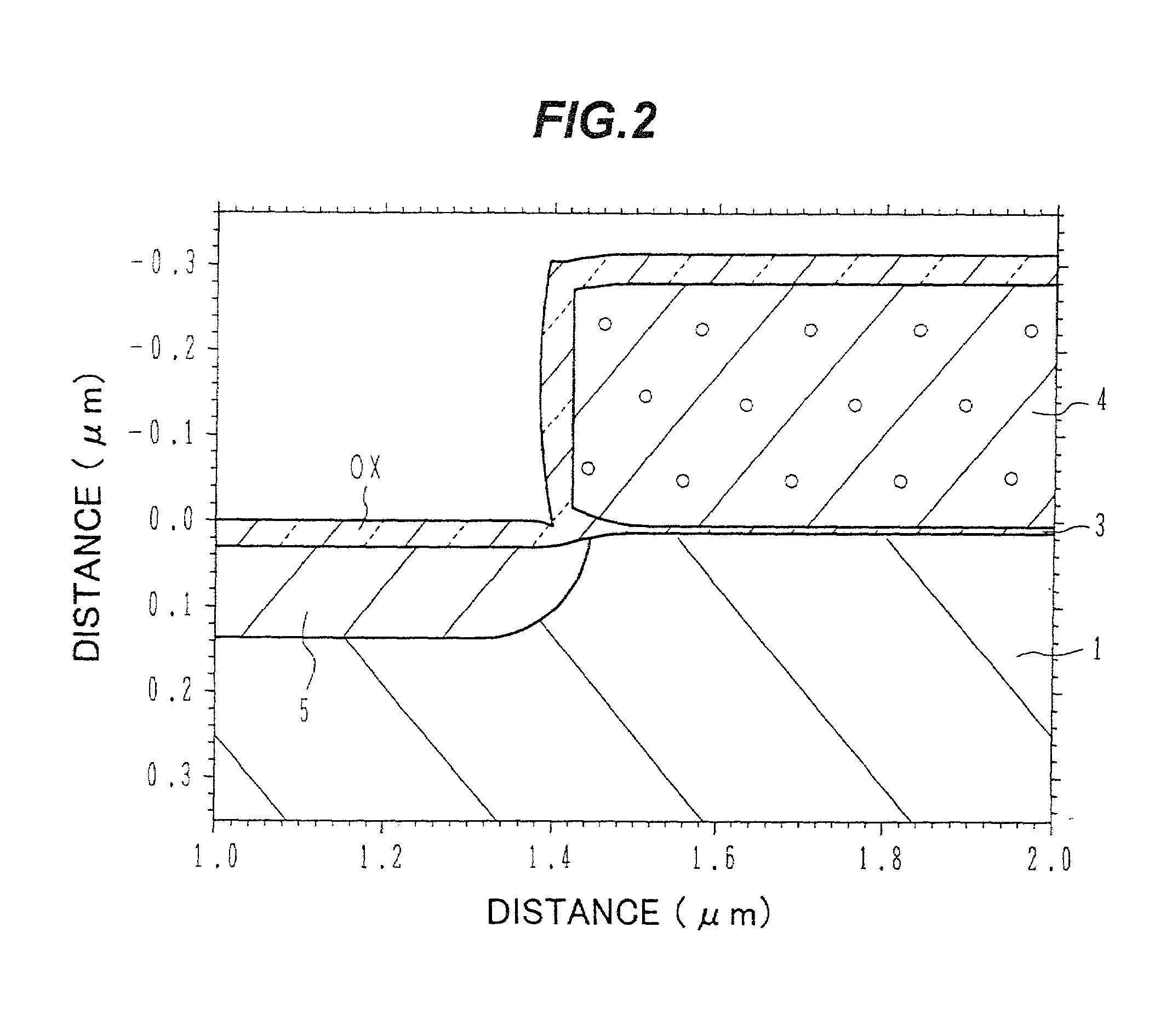
[0022]FIGS. 1A–1D are schematic sectional views of MOS transistors in a multi-voltage level semiconductor device according to an embodiment of the present invention.

[0023]In FIG. 1A, a MOS transistor for a low-voltage circuit is shown on the left-hand side, and a MOS for a high-voltage circuit is shown on the right-hand side. For example, a field oxide film 2 is formed onto the surface of a silicon substrate 1, to define or demarcate active regions. Gate oxide films 3 are then formed onto the surface of the active regions. Here the thickness of the gate oxide film 3 gradually decreases from the edges 3b towards the centre 3a of the film, with respect to the direction in which current flows through the MOS transistor.

[0024]Polycrystalline silicon electrodes 4a, and 4b are formed onto the gate oxide films 3. The polycrystalline silicon electrode 4a for a low-voltage circuit is doped with a higher concentration of impurity than the polycrystalline silicon electrode 4b for the high-volt...


PUM


Abstract

In a semiconductor device comprising a MOS transistor driven at a relatively low voltage and a MOS transistor driven at a relatively high voltage formed on the same semiconductor substrate, the MOS transistor driven at the relatively high voltage comprises: a first active region of a first conductivity type in the semiconductor substrate; a first gate oxide film formed on the first active region and having increased thickness at the edge regions thereof than in the central region thereof in the direction of current flow; and a first electrode formed on the first gate oxide film and doped at a relatively low concentration with an impurity of a second conductivity type which is opposite to the first conductivity type; and the MOS transistor driven at the relatively low voltage comprises: a second active region of a first conductivity type in the semiconductor substrate; a second gate oxide film formed on the second active region; and a second electrode formed on the second gate oxide film and doped at a relatively high concentration with an impurity of a second conductivity type.
A multi-voltage level semiconductor device is provided whereby increases in the number of manufacturing steps can be restricted and decline in the performance of MOS transistors for use in low-voltage circuits can be suppressed.

Description

[0001]This application is a divisional of Ser. No. 09 / 021,519 filed Feb. 10, 1998, now U.S. Pat. No. 6,271,572 which is based on Japanese patent application No. 9-28132, filed Feb. 12, 1997, the whole contents of which are incorporated herein by reference.BACKGROUND OF THE INVENTION[0002]a) Field of the Invention[0003]The present invention relates to a semiconductor device and a method of manufacturing same, and more particularly, to a semiconductor device handling a plurality of voltage levels, and a method of manufacturing same.[0004]b) Description of the Related Art[0005]Drive voltages for semiconductor integrated circuits have tended to fall as savings in power consumption are made. For example, analogue circuits, such as a TTL, have been developed with a 5V power source, but subsequently developed digital circuits are generally driven at 3.3 V. The drive power supply for digital circuits has been tending to fall even further, to 2.5V. In memory devices, and the like, even more ...

Claims


Application Information

Patent Timeline
IPC IPC(8): H01L21/8234H01L29/78H01L27/088
CPCH01L21/8234
Inventor FUJITA, HARUMITSU
Owner YAMAHA CORP
Why Eureka
Try Eureka