

Package structure and forming method of the same
- Summary
- Abstract
- Description
- Claims
- Application Information
AI Technical Summary
Benefits of technology
Problems solved by technology
Method used
Image

Examples
Embodiment Construction
[0041]Reference will now be made in detail to the present embodiments of the invention, examples of which are illustrated in the accompanying drawings. Wherever possible, the same reference numbers are used in the drawings and the description to refer to the same or like parts.
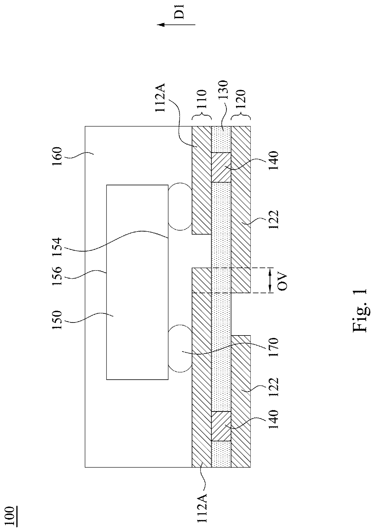
[0042]FIG. 1 is a cross-sectional view of a package structure 100 according to some embodiments of the present disclosure. The package structure 100 includes a first conduction layer 110, a second conduction layer 120, and an isolation layer 130. The first conduction layer 110 has a plurality of first portions 112A. The second conduction layer 120 has a plurality of portions 122. The first portions 112A of the first conduction layer 110 are electrically insulated and spaced apart from each other, and the portions 122 of the second conduction layer 120 are electrically insulated and spaced apart from each other. The isolation layer 130 is disposed between the first conduction layer 110 and the second conduction...
PUM
 Abstract
Description
Claims
Application Information