High ruggedness heterojunction bipolar transistor structure

Active Publication Date: 2020-05-21
VISUAL PHOTONICS EPITAXY
View PDF8 Cites 0 Cited by
  • Summary
  • Abstract
  • Description
  • Claims
  • Application Information

AI Technical Summary

Benefits of technology

[0005]Based on the above technical issues, the present invention provides a high ruggedness heterojunction bipolar transistor structure. In addition to effectively increasing the breakdown voltage of the emitter-base junction and reducing the emitter-base junction capacitance without increasing or with slightly increasing the emitter resistance, the structure can also use the aluminum-containing (Al) semiconductor material such as AlGaAs, which has a high bandgap and the resistivity

Problems solved by technology

However, when the HBT operates at a high voltage or a high current, the HBT is prone to damage due to excessive power.
For example, the excessive power rebounded back when the PA is not in the impedance match condition and causes the ruggedness issue of the PA.
However, when a highly doped emitter cap layer 60 is used, the breakdown voltage (BVebo) of the emitt

Method used


Image

  • High ruggedness heterojunction bipolar transistor structure
  • High ruggedness heterojunction bipolar transistor structure
  • High ruggedness heterojunction bipolar transistor structure

Examples


Embodiment Construction

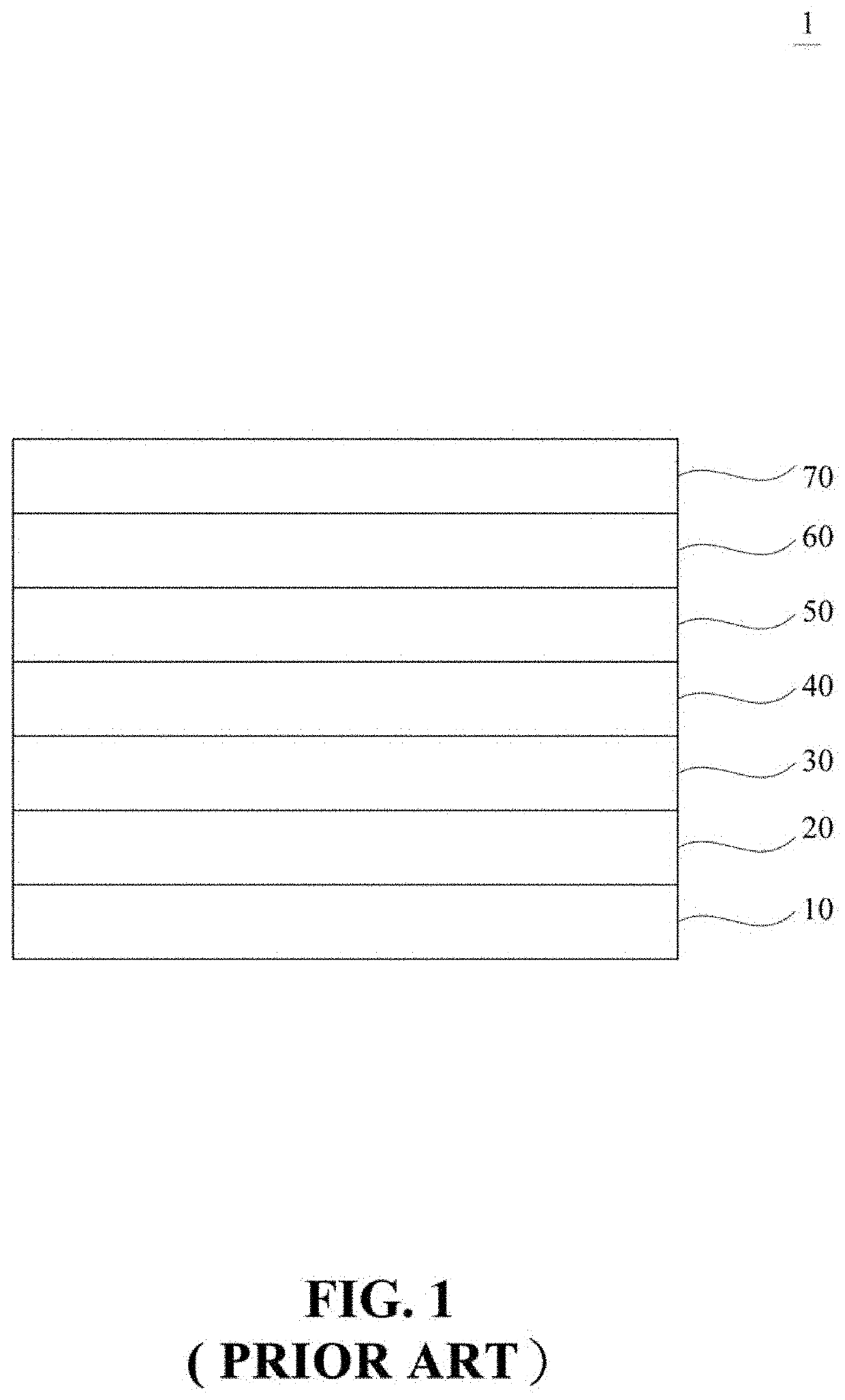
[0032]In the following detailed description, for purpose of explanation, numerous specific details are set forth in order to provide a thorough understanding of the disclosed embodiments. It will be apparent, however, that one or more embodiments may be practiced without these specific details. In other instances, well-known structures and devices are schematically shown in order to simplify the drawing.

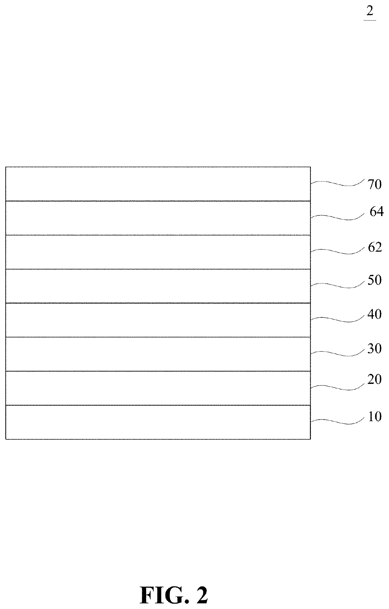
[0033]FIG. 2 shows a schematic view of a high ruggedness heterojunction bipolar transistor (HBT) structure in accordance with an exemplary embodiment of the present invention. As shown in FIG. 2, the HBT structure 2 comprises: a substrate 10, a sub-collector layer 20, a collector layer 30, a base layer 40, an emitter layer 50, a first emitter cap layer 62, a second emitter cap layer 64 and an ohmic contact layer 70.

[0034]In the HBT structure 2, the sub-collector layer 20 is stacked on the substrate 10 and formed of an N-type III-V semiconductor material; the collector layer 30 is sta...


PUM


Abstract

The disclosure provides a high ruggedness HBT structure, including: a sub-collector layer on a substrate and formed of an N-type III-V semiconductor material; a collector layer on the sub-collector layer and formed of a III-V semiconductor material; a base layer on the collector layer and formed of a P-type III-V semiconductor material; an emitter layer on the base layer and formed of one of N-type semiconductor materials of InGaP, InGaAsP and InAlGaP; a first emitter cap layer on the emitter layer and formed of one of undoped or N-type semiconductor materials of AlxGa1-xAs, AlxGa1-xAs1-yNy, AlxGa1-xAs1-zPz, AlxGa1-xAs1-wSbw, and InrAlxGa1-x-rAs, x having a highest value between 0.05≤x≤0.4, and y, z, r, w≤0.1; a second emitter cap layer on the first emitter cap layer and formed of an N-type III-V semiconductor material; and an ohmic contact layer on the second emitter cap layer and formed of an N-type III-V semiconductor material.

Description

CROSS-REFERENCE TO RELATED APPLICATION[0001]This application claims the priority of Taiwanese patent application No. 107141339, filed on Nov. 20, 2018, which is incorporated herewith by reference.BACKGROUND OF THE INVENTION1. Field of the Invention[0002]The technical field generally relates to a high ruggedness heterojunction bipolar transistor structure, in particular, to adding a first emitter cap layer containing Al over the emitter layer of the heterojunction bipolar transistor; the first emitter cap layer being formed of at least one of undoped or N-type semiconductor materials of AlxGa1-xAs, AlxGa1-xAs1-yNy, AlxGa1-xAs1-zPz, AlxGa1-xAs1-wSbw, and InrAlxGa1-x-rAs, x having a highest value between 0.05≤x≤0.4, and y, z, r, w≤0.1.2. The Prior Arts[0003]The heterojunction bipolar transistors (HBTs) use different semiconductor materials to form the emitter and the base layers, and form a heterojunction at the junction of the emitter and the base. The advantage is that the emitter in...

Claims


Application Information

Patent Timeline
IPC IPC(8): H01L29/08H01L33/00H01L29/737H01L29/205
CPCH01L29/205H01L33/0025H01L29/7371H01L29/0817H01L29/7785H01L33/30H01L33/32H01L29/66318H01L29/0804H01L27/0823H01L29/0821H01L29/7375H01L29/732
Inventor CHIN, YU-CHUNGHUANG, CHAO-HSINGTSENG, MIN-NANCHEN, KAI-YU
Owner VISUAL PHOTONICS EPITAXY
Why Eureka
Try Eureka