Electron mobility enhancement for MOS devices with nitrided polysilicon re-oxidation

Inactive Publication Date: 2008-05-29
TAIWAN SEMICON MFG CO LTD
View PDF5 Cites 10 Cited by
  • Summary
  • Abstract
  • Description
  • Claims
  • Application Information

AI Technical Summary

Problems solved by technology

The patterning of the gate stack may cause damage to the gate electrode and gate dielectric, and thus adversely affects the integrity of gate dielectric.
One of the consequences is that in regions of the gate dielectric close to bottom corners of the gate electrode, a high electrical field may exist, and the adversely affected gate dielectric will cause reliability problems.
In addition, the leakage

Method used


Image

  • Electron mobility enhancement for MOS devices with nitrided polysilicon re-oxidation
  • Electron mobility enhancement for MOS devices with nitrided polysilicon re-oxidation
  • Electron mobility enhancement for MOS devices with nitrided polysilicon re-oxidation

Examples


first embodiment

[0022]In a first embodiment, nitrided polysilicon re-oxidation layer 28 is formed by performing an oxidation step to form an oxide layer on the surface of substrate 20 and sidewalls of the gate stacks, and then nitridating the oxide layer to form nitrided polysilicon re-oxidation layer 28. The oxide layer may be formed by a rapid thermal oxidation (RTO), a furnace dry oxide anneal, or other commonly used oxidation methods. Preferably, the oxide layer is formed at an elevated temperature, for example, between about 400° C. and about 1100° C. in an environment comprising oxygen-containing gases. The preferred oxygen-containing gases may include O2, NO, N2O, NO2, O3, H2O, a combined gas of H2 and O2, and combinations thereof.

[0023]A nitridation is then performed to the oxide layer to convert the oxide layer to nitrided polysilicon re-oxidation layer 28. In the preferred embodiment, plasma nitridation is performed, wherein the process gases may include nitrogen-containing gases, such as...

second embodiment

[0024]In a second embodiment, the re-oxidation and nitridation are performed simultaneously. Preferably, the process gases include both oxygen and nitrogen containing gases, such as oxygen, NO, N2O, NO2, NH3, NO-based gases such as NO, N2O, NO2, and combinations thereof. Similarly, the simultaneous re-oxidation and nitridation may be performed with the assistance of plasma or under thermal conditions.

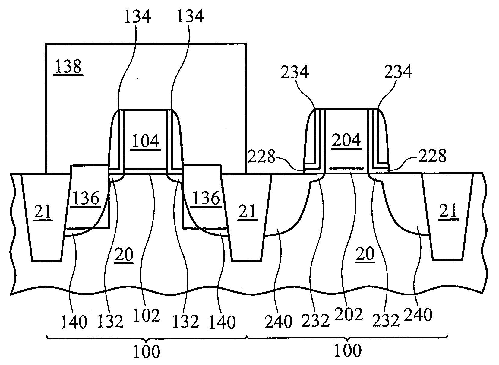
[0025]Referring to FIG. 5, photo resist 130 is formed and patterned to mask PMOS region 100. Lightly-doped drain / source (LDD) regions 232 and pocket regions (not shown) are then formed. As is known in the art, to form LDD regions 232, an implantation is performed to introduce n-type impurities into substrate 20 to form LDD regions 232. The implanted impurities penetrate nitrided re-oxidation layer 228 into substrate 20. Pocket regions are also formed by implanting p-type impurities. Photo resist 130 is then removed.

[0026]Referring to FIG. 6, photo resist 230 is formed and patterned to m...


PUM


Abstract

A semiconductor structure includes a PMOS device and an NMOS device. The PMOS device includes a first gate dielectric on a semiconductor substrate, a first gate electrode on the first gate dielectric, and a first gate spacer along sidewalls of the first gate electrode and the first gate dielectric. The NMOS device includes a second gate dielectric on the semiconductor substrate, a second gate electrode on the second gate dielectric, a nitrided polysilicon re-oxidation layer having a vertical portion and a horizontal portion wherein the vertical portion is on sidewalls of the second gate electrode and the second gate dielectric and wherein the horizontal portion is on the semiconductor substrate, and a second gate spacer on sidewalls of the second gate electrode and the second gate dielectric, wherein the second gate spacer is on the horizontal portion of the nitrided polysilicon re-oxidation layer.

Description

TECHNICAL FIELD[0001]This invention relates generally to semiconductor devices, and more particularly to structures and manufacturing methods of metal-oxide-semiconductor devices.BACKGROUND[0002]Polysilicon gates are widely used in the manufacture of metal-oxide-semiconductor (MOS) devices. In typical polysilicon (polysilicon) gate formation processes, after the formation of a gate dielectric layer and a polysilicon layer, the gate dielectric layer and the polysilicon layer are patterned to form a gate stack, which includes a gate electrode on a gate dielectric.[0003]The patterning of the gate stack may cause damage to the gate electrode and gate dielectric, and thus adversely affects the integrity of gate dielectric. One of the consequences is that in regions of the gate dielectric close to bottom corners of the gate electrode, a high electrical field may exist, and the adversely affected gate dielectric will cause reliability problems. In addition, the leakage current between the ...

Claims


Application Information

Patent Timeline
IPC IPC(8): H01L21/8238
CPCH01L21/28247H01L29/6656H01L29/66545H01L21/823864
Inventor LIN, WENLILEE, DA-YUANCHEN, CHI-CHUNCHEN, SHIH-CHANG
Owner TAIWAN SEMICON MFG CO LTD
Why Eureka
Try Eureka