Semiconductor device carrying micro electro mechanical system

Inactive Publication Date: 2008-06-05
HITACHI LTD
View PDF14 Cites 39 Cited by
  • Summary
  • Abstract
  • Description
  • Claims
  • Application Information

AI Technical Summary

Benefits of technology

[0015]Thus, the present invention allows an MEMS sensor formed on a semiconductor integrated circuit device to have high reliability by hermetically sealing the MEMS sensor portion with passivation films. Further, the prese

Problems solved by technology

However, such a conventional technique is disadvantageous in that the sensor may exhibit drift in characteristics.
Another reason is degradation of the quality of the films making up the MEMS sensor.
However, such an arrangement is difficult to apply to MEMS sensors, si

Method used


Image

  • Semiconductor device carrying micro electro mechanical system
  • Semiconductor device carrying micro electro mechanical system
  • Semiconductor device carrying micro electro mechanical system

Examples


Example

First Embodiment

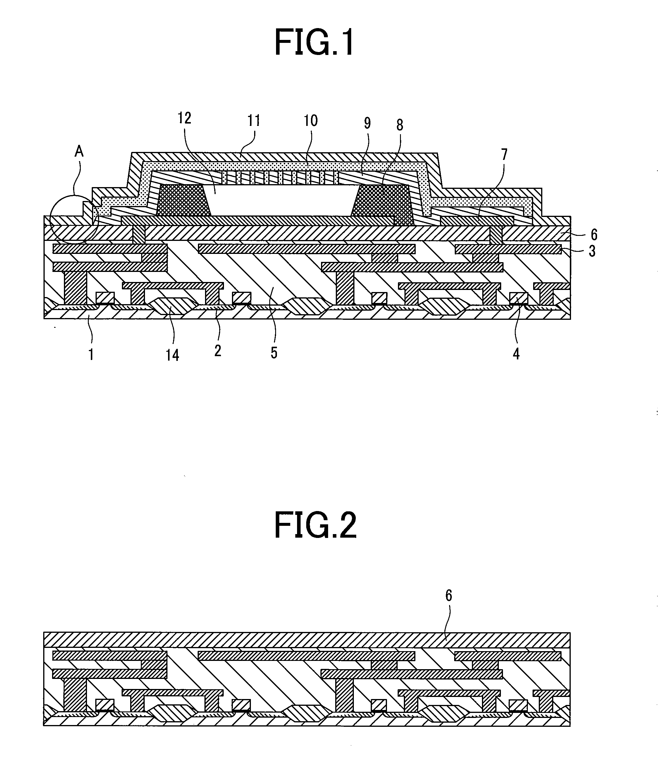
[0021]A first embodiment of the present invention will be described with reference to a capacitive MEMS pressure sensor formed on the top wiring layer of a semiconductor integrated circuit device. FIG. 1 is a cross-sectional view of the MEMS pressure sensor. As shown in FIG. 1, a lower passivation film layer 6 is provided on the surface of the wiring layer of a semiconductor integrated circuit device formed on a semiconductor substrate, and the pressure sensor is provided on the lower passivation film layer 6. The pressure sensor includes a lower electrode layer 7 (formed on the lower passivation layer 6) and an upper electrode layer 9, which together form a capacitance. The cavity 12 between the lower electrode layer 7 and the upper electrode layer 9 is sealed by an insulating sealing film layer 10 and an upper passivation film 11. The cavity 12 permits the upper electrode layer 9 to be deformed under external pressure, which results in a change in the capacitance b...

Example

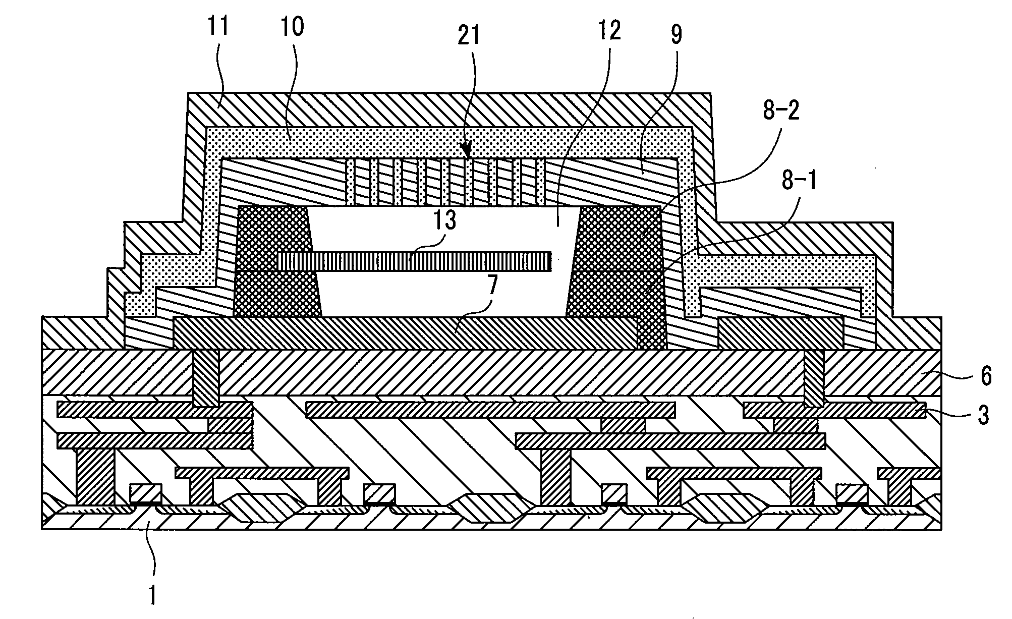
[0031]A second embodiment of the present invention is directed to MEMS structures with a cavity other than pressure sensors. The present embodiment will be described with reference to a capacitive MEMS acceleration sensor formed on the top wiring layer of a semiconductor integrated circuit device. FIG. 11 is a cross-sectional view of this acceleration sensor. The acceleration sensor shown in FIG. 11 includes a moving electrode layer 13 designed to be able to be deformed even by small force, as in the pressure sensor of the first embodiment. This allows the acceleration sensor to sense an acceleration applied thereto by sensing the resultant movement (or deformation) of the moving electrode layer 13. There will now be described a process for manufacturing the MEMS structure (or capacitive MEMS acceleration sensor) of the present embodiment. After forming integrated circuit wiring 3 on a semiconductor integrated circuit substrate 1 (see FIG. 11), the surface of the substrate 1 is plan...


PUM


Abstract

An object of the present invention is to enhance the reliability of an MEMS sensor formed on a semiconductor integrated circuit device.
To achieve this object, a semiconductor device of the present invention comprises: a semiconductor integrated circuit device; a lower passivation film of silicon nitride, etc. formed on the semiconductor integrated circuit device and having high moisture resistance and high chemical resistance; an MEMS portion formed on the lower passivation film and including a cavity 12; and an upper passivation film 11 formed on the top surface of the MEMS portion such that the MEMS portion is hermetically sealed by the upper and lower passivation films.

Description

CLAIM OF PRIORITY[0001]The present application claims priority from Japanese application JP 2006-323865 filed on Nov. 30, 2006, the content of which is hereby incorporated by reference into this application.BACKGROUND OF THE INVENTION[0002]1. Field of the Invention[0003]The present invention relates to a semiconductor device that includes a sensor formed by use of an MEMS (Micro-Electro-Mechanical System) technique, and more particularly relates to a technique for enhancing the reliability of sensors.[0004]2. Description of the Related Art[0005]One conventional method for enhancing the reliability of a sensor formed by an MEMS technique is, for example, to passivate its top surface by forming a silicon nitride film, as disclosed in Japanese Patent Laid-Open No. 2006-156. Specifically, according to the technique disclosed in this publication, a capacitive MEMS pressure sensor having a moving electrode (or a diaphragm electrode) and an opposing fixed electrode is formed on the top wir...

Claims


Application Information

Patent Timeline
IPC IPC(8): H01L29/84
CPCB81B7/0058B81B2201/0235B81C2203/0136B81B2207/015B81B2201/0264
Inventor FUJIMORI, TSUKASAHANAOKA, YUKOFUKUDA, HIROSHI
Owner HITACHI LTD
Why Eureka
Try Eureka