Thin film transistor substrate and method of manufacture

a thin film transistor and substrate technology, applied in the field of liquid crystal display devices, can solve the problems of high defect rate of slit masks, difficult to form uniform channels of less than 3 m using slit masks, and high cost of slit masks, so as to reduce the size of pixel tft, prevent defects of channel area, and improve the aperture ratio

Active Publication Date: 2008-06-12
KLA TENCOR TECH CORP +1
View PDF11 Cites 74 Cited by
  • Summary
  • Abstract
  • Description
  • Claims
  • Application Information

AI Technical Summary

Benefits of technology

[0011]The present invention provides a thin film transistor (“TFT”) substrate in which a channel of a pixel TFT is formed using a single slit

Problems solved by technology

However, the slit mask and the halftone mask are expensive and the slit mask has a high defect rate due to differences in the amount

Method used


Image

  • Thin film transistor substrate and method of manufacture
  • Thin film transistor substrate and method of manufacture
  • Thin film transistor substrate and method of manufacture

Examples


first embodiment

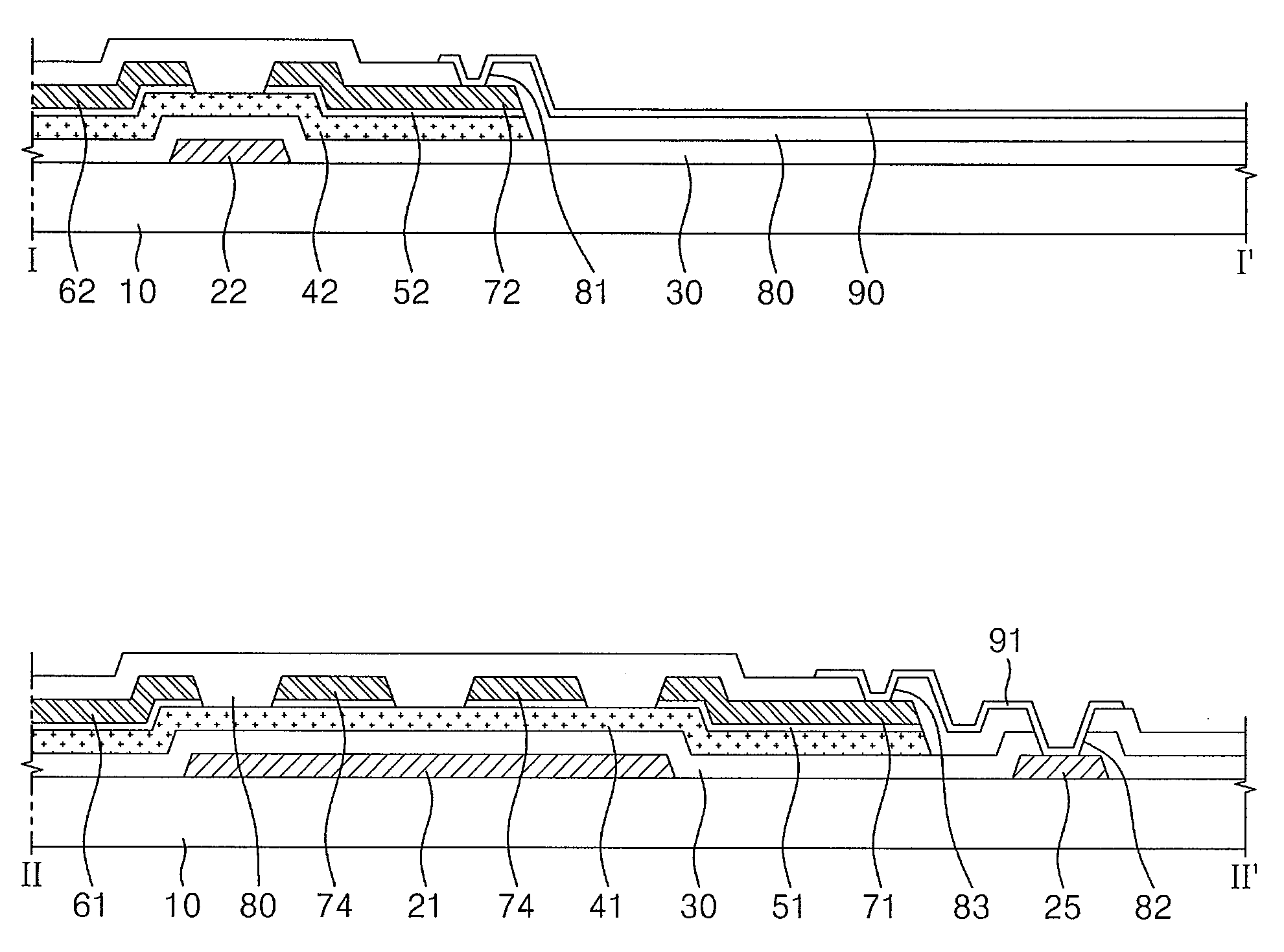
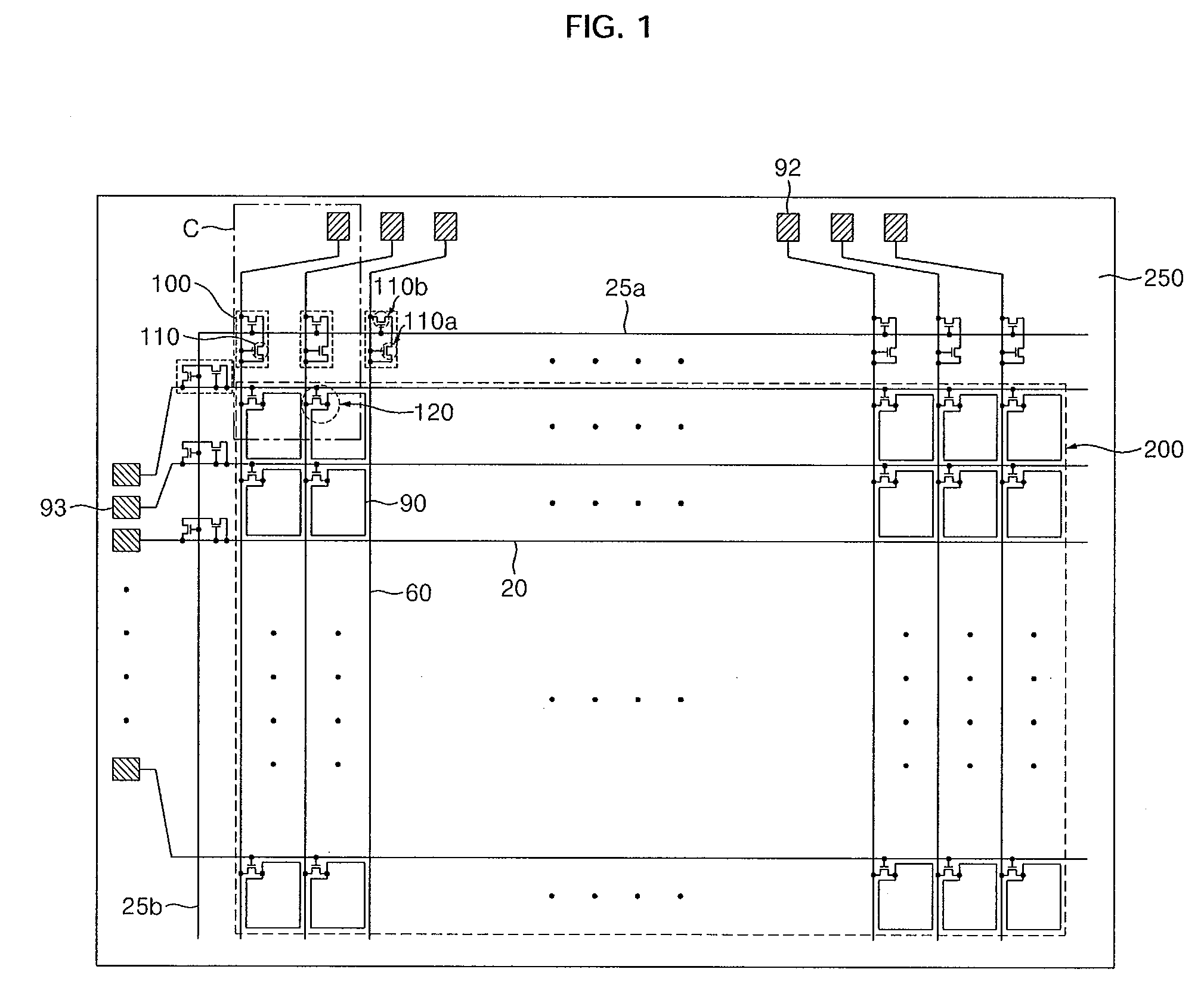
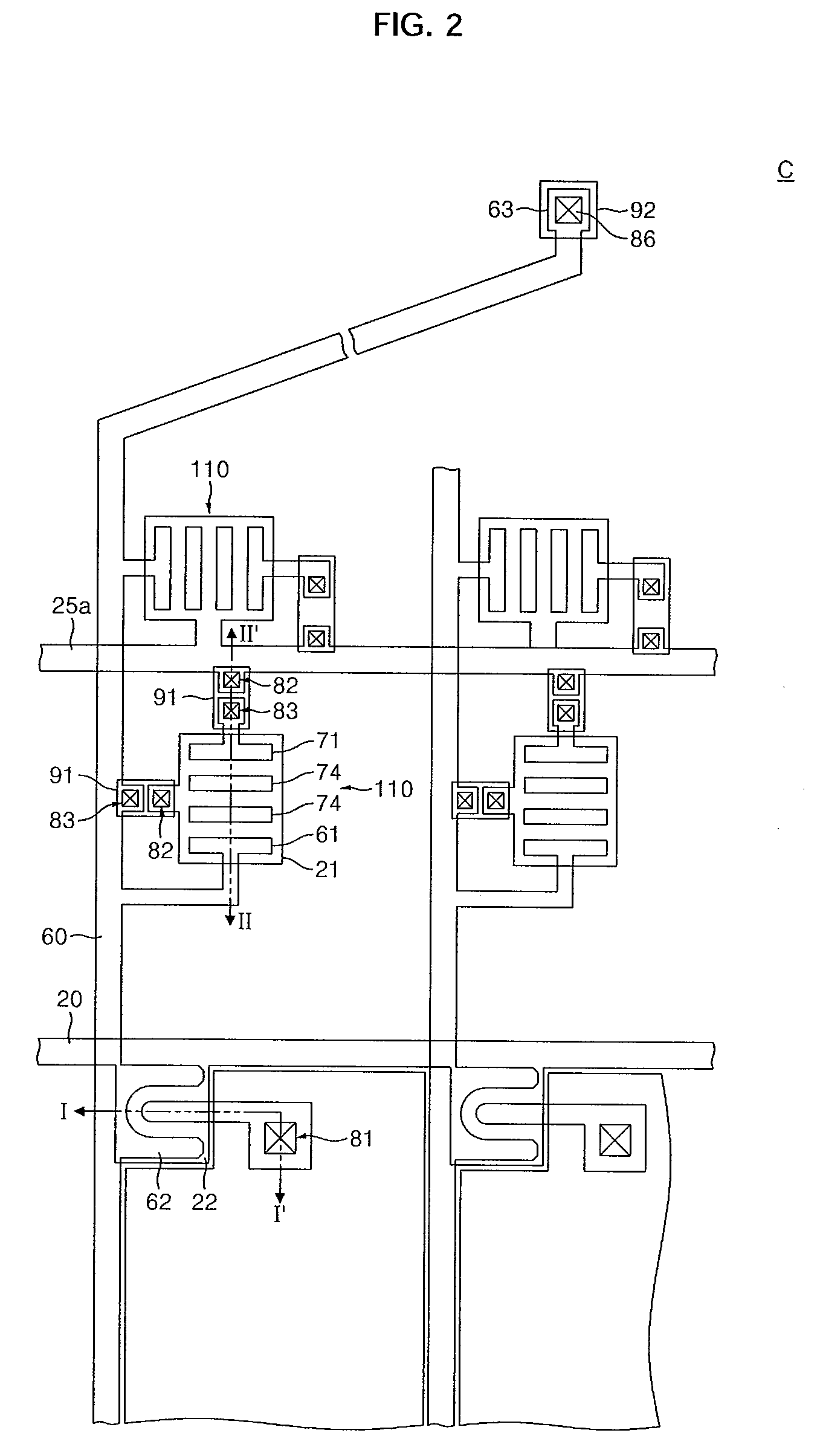
[0037]FIG. 1 is a plan view showing a thin film transistor (“TFT”) substrate in accordance with the present invention, FIG. 2 is an enlarged view of area C shown in FIG. 1, and FIG. 3 is a cross-sectional view taken along lines I-I′ and II-II′ of the TFT substrate shown in FIG. 2.

[0038]Referring to FIGS. 1, 2, and 3, a TFT substrate 10 in accordance with a first embodiment of the present invention includes a display area 200 and a non-display area 250 surrounding the display area 200. The display area 200 includes a gate line 20 and a data line 60 which are insulated from each other, a pixel TFT 120 electrically connected to the gate line 20 and the data line 60, and a pixel electrode 90 connected to the pixel TFT 120.

[0039]The non-display area 250 includes a signal supply pad including a gate pad 93 and a data pad 92 formed at each end of the gate line 20 and the data line 60 to receive signals from the outside, a discharge line 25 formed between the signal supply pad and the displ...

second embodiment

[0056]FIG. 6 is a plan view showing a TFT substrate in accordance with the present invention.

[0057]As shown in FIG. 6 in comparison with FIG. 2, the test line 26 is formed in the non-display area 250 of the substrate 10, and the ESD protection circuit 100 is provided between the test line 26 and the gate pad 93 and between the test line 26 and a data pad 92, respectively.

[0058]The test line 26 includes a data test line 26a applying a data test signal to the data line 60, and a gate test line 26b applying a gate test signal to the gate line 20. The data test line 26a is connected to the data pad 92, and the gate test line 26b is connected to the gate pad 93. A data test pad 94 applying the data test signal is formed on one end of the data test line 26a, and a gate test pad 95 applying the gate test signal is formed on one end of the gate test line 26b. A test voltage applied to the gate test pad 95 and the data test pad 94 to test the TFT substrate is input through a separate probe. ...


PUM


Abstract

A thin film transistor (“TFT”) substrate in which the size of a pixel TFT formed in a display area is reduced using a single slit mask, and the length of the channel area of a protection TFT constituting an electrostatic discharge protection circuit formed in a non-display area is formed larger than that of the pixel TFT using the same mask pattern. The TFT substrate includes a signal line and a discharge line formed on a substrate, a signal supply pad formed on one end of the signal line to supply a signal to the signal line, and an electrostatic discharge protection circuit including at least one protection TFT including a plurality of channels formed between the signal supply pad and the discharge line and/or between the signal line and the discharge line.

Description

CROSS-REFERENCE TO RELATED APPLICATION(S)[0001]The present application claims priority to Korean Patent Application No. 2006-0125950, filed on Dec. 12, 2006, the disclosure of which is incorporated herein by reference in its entirety.BACKGROUND OF THE INVENTION[0002]1. Field of the Invention[0003]The present disclosure relates to a liquid crystal display device and, more particularly, to a device having an improved thin film transistor (“TFT”) substrate.[0004]2. Description of the Related Art[0005]A liquid crystal display (“LCD”) device includes a liquid crystal panel displaying an image, a panel driving unit driving the liquid crystal panel, and a light source providing light to the liquid crystal panel. The panel driving unit includes a gate driving unit driving gate lines and a data driving unit driving data lines. The gate driving unit supplies a scan signal to the gate lines sequentially, and the data driving unit supplies a data voltage to the data lines when the scan signal i...

Claims


Application Information

Patent Timeline
IPC IPC(8): H01L27/12H01L21/84
CPCH01L27/0248H01L27/1288H01L27/1214G02F1/136204H01L27/12
Inventor SHIN, KYOUNG-JUCHAI, CHONG-CHULJUNG, MEE-HYE
Owner KLA TENCOR TECH CORP
Why Eureka
Try Eureka