FinFET and method of manufacturing the same

a technology of micro-fluidic transistors and transistors, which is applied in the direction of micro-fluidic transistors, basic electric elements, electrical apparatus, etc., can solve the problems of insufficient performance of mos devices having a channel length of near 30 nm, and the need for devices to shrink,

Inactive Publication Date: 2008-06-12
SAMSUNG ELECTRONICS CO LTD
View PDF6 Cites 51 Cited by
  • Summary
  • Abstract
  • Description
  • Claims
  • Application Information

AI Technical Summary

Benefits of technology

[0009]Embodiments are therefore directed to a semiconductor device and a method o...

Problems solved by technology

With the downscaling of systems using silicon semiconductor technology and the increased demand for low power consumption, devices also need to shrink.
Presently, the on-going downscaling in the gate size of devices gives rise to problems with, especially, a short channel effect (SCE).
A MOS device having a channel length of near 30 nm may still be insufficient for an actual circuit in terms of performance.
Furthermore, an area occupied by a single actual device does not shrink due to an unreduced space region formed beside a gate,...

Method used


Image

  • FinFET and method of manufacturing the same
  • FinFET and method of manufacturing the same
  • FinFET and method of manufacturing the same

Examples


Embodiment Construction

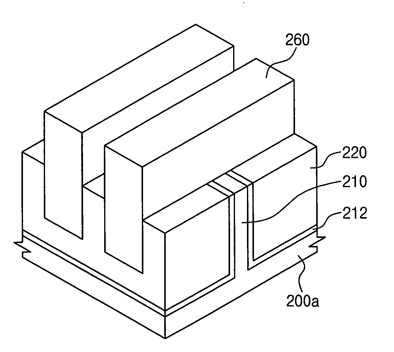
[0025]Korean Patent Application 2006-124950, filed on Dec. 8, 2006, in the Korean Intellectual Property Office, and entitled: “FinFET and Method of Manufacturing the Same,” is incorporated by reference herein in its entirety.

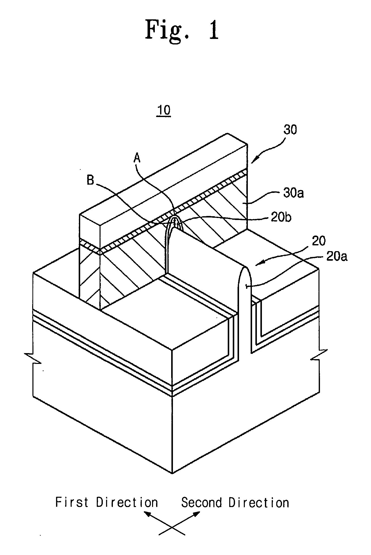
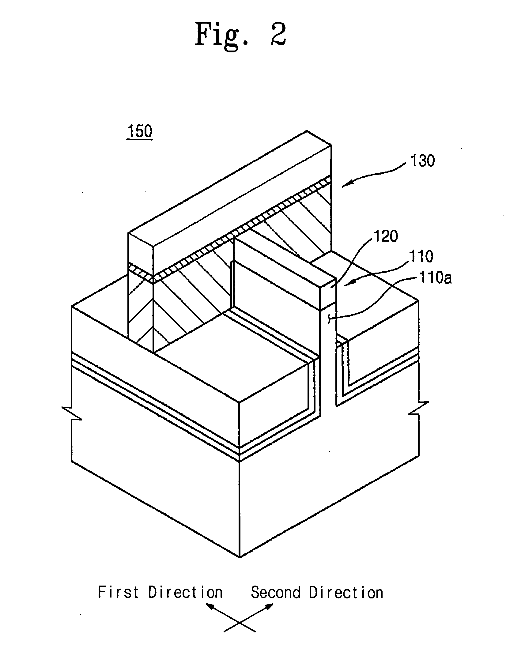
[0026]Embodiments will now be described more fully hereinafter with reference to the accompanying drawings, in which example embodiments are illustrated. This invention, however, may be embodied in many different forms and should not be construed as limited to the embodiments set forth herein. Rather, these embodiments are provided so that this disclosure will be thorough and complete, and will fully convey the scope of the invention to those skilled in the art. In the drawings, the thicknesses of layers and regions are exaggerated for clarity. It will also be understood that when a layer is referred to as being on or under another layer or substrate, it may be directly on or under the other layer or substrate, or intervening layers may also be present. Like num...


PUM


Abstract

A FinFET may include a semiconductor fin having a top surface and a sidewall having different crystal planes. A gate dielectric layer on the top surface and on the sidewall has different thicknesses. A gate electrode is formed on the gate dielectric layer across the top surface and sidewall of the semiconductor fin.

Description

BACKGROUND[0001]1. Field of the Invention[0002]Embodiments relate to a semiconductor device and a method of manufacturing the same. More particularly, embodiments relate to a fin field effect transistor (FinFET) and a method of manufacturing the same.[0003]2. Description of the Related Art[0004]A vast amount of research has lately been conducted on nano-CMOS device technology worldwide because the nano-CMOS device technology can be applied to logic circuits, such as a central processing unit (CPU), and memories to create high value-added products. With the downscaling of systems using silicon semiconductor technology and the increased demand for low power consumption, devices also need to shrink. Presently, the on-going downscaling in the gate size of devices gives rise to problems with, especially, a short channel effect (SCE).[0005]Conventional CMOS technology involves forming CMOS devices on a bulk silicon substrate. When a MOS device formed on a bulk silicon substrate has a gate...

Claims


Application Information

Patent Timeline
IPC IPC(8): H01L29/04H01L21/336
CPCH01L29/045H01L29/785H01L29/66795H01L21/18
Inventor LEE, DEOK-HYUNGLEE, SUN-GHILYOO, JONG-RYEOLCHOI, SI-YOUNG
Owner SAMSUNG ELECTRONICS CO LTD
Why Eureka
Try Eureka