Lead frame

a lead frame and frame technology, applied in the field of lead frame, can solve the problems of electrical damage, possible cut in the bonding wire, and the risk of each stage unit deformation in the following process, so as to reduce the stress on the connecting unit, reduce the risk of deformation of each stage unit, and reduce the risk of peeling off of the connecting unit

Inactive Publication Date: 2008-06-12
YAMAHA CORP
View PDF2 Cites 7 Cited by
  • Summary
  • Abstract
  • Description
  • Claims
  • Application Information

AI Technical Summary

Benefits of technology

[0017]In each stage unit the angled part opposing to the part connected to the support unit is a free edge and moves largely when deformed. By connecting the angle parts with the connecting unit, the plurality of the stage units are united and deformation is reduced. Therefore, the plurality of the stage units can be stably supported. Moreover, stress to the connectin...

Problems solved by technology

When the plurality of the stage units are equipped, there is a risk for each stage unit to be deformed in following processes such as a packaging process, etc.
If the stage is buffeted, an electrical damage such as cut in a bonding wire may occur.
As a result, it may caus...

Method used


Image

  • Lead frame
  • Lead frame
  • Lead frame

Examples


first embodiment

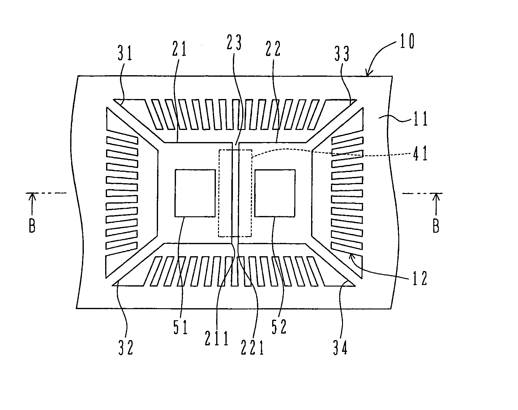
[0030]In case of the present invention, the two stage units 21 and 22 are positioned approximately on the same plane. Therefore, the semiconductor chip 51 mounted on the stage unit 21 and the semiconductor chip 52 mounted on the stage unit 22 are mounted on the approximately same plane. The semiconductor chips 51 and 52 which are mounted on the stage unit 21 and the stage unit 22 are electrically connected with the inner lead 12 in the following bonding process.

[0031]A connecting tape 41 is positioned between the stage unit 21 and the stage unit 22. The connecting tape 41 includes, for example, a base composed of resin and an adhering part applied at least on one surface of the base. The base of the connecting tape 41 is formed with resin with high insulation and heat-resistance. The connecting tape 41 certainly connects between the stage unit 21 and the stage unit 22 in a packaging process by forming the base of the connecting tape 41 with the resin with high heat-resistance. For e...

second embodiment

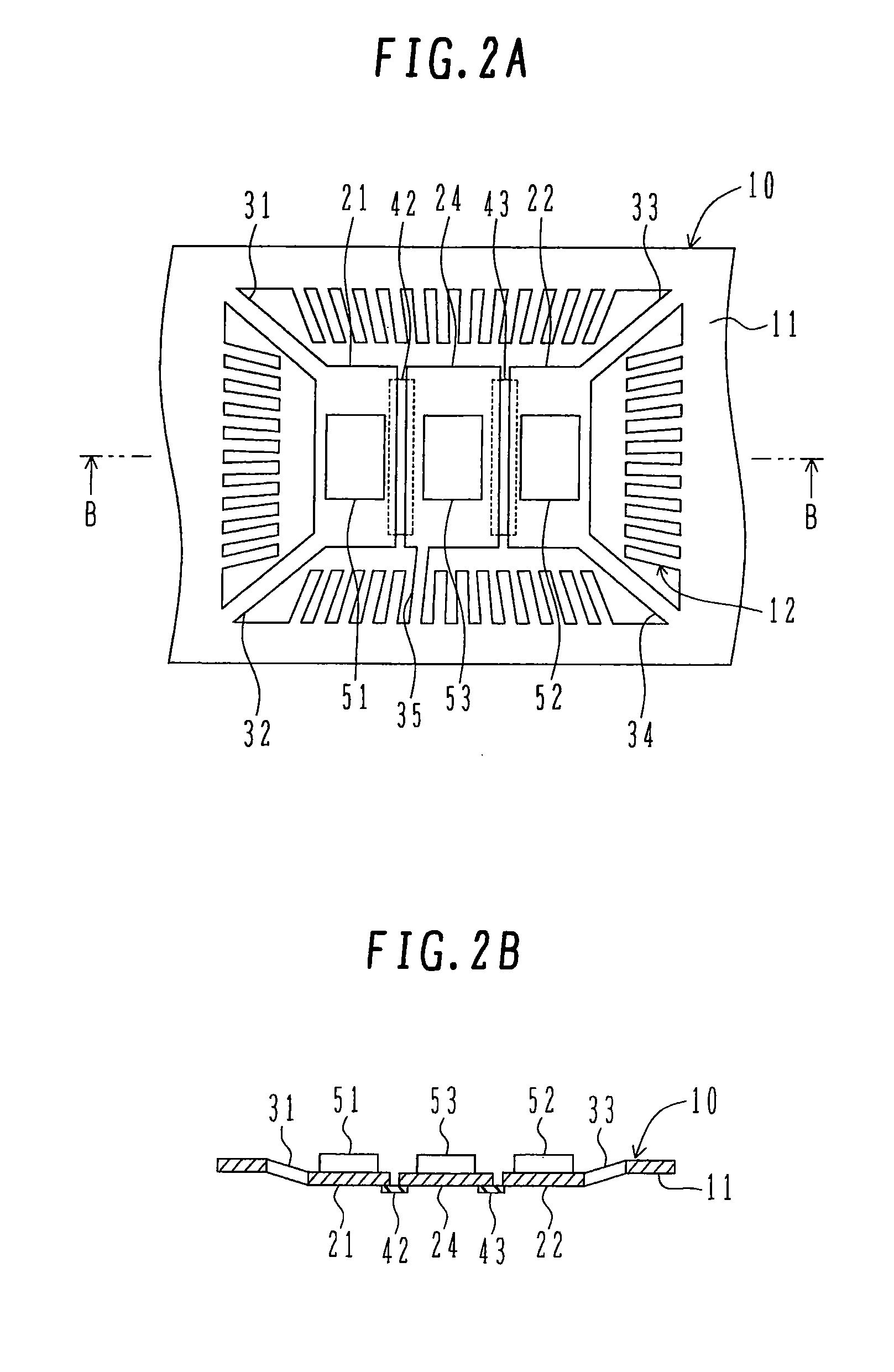
[0038]In case of the second embodiment shown in FIG. 2A and FIG. 2B, the lead frame 10 equips with three stage units 21, 22 and 24. The stage unit 21 is supported on the frame unit 11 by the supporting units 31 and 32. The stage unit 22 is supported on the frame unit 11 by the supporting units 33 and 34. The stage unit 24 is supported on the frame unit 11 by the supporting unit 35. The semiconductor chip 51, the semiconductor chip 52 and the semiconductor chip 53 are respectively mounted on the stage unit 21, the stage unit 22 and the stage unit 24.

[0039]The stage unit 21 and the stage unit 24 are connected by a connecting tape 42, and the stage unit 24 and the stage unit 22 are connected by a connecting tape 43. By that, the stage unit 21, the stage unit 22 and the stage unit 24 are unitedly connected.

[0040]In the second embodiment, deformation of the stage unit 21, the stage unit 22 and the stage unit 24 can be reduced even though the lead frame 10 equips with three stage units 21...

third embodiment

[0042]In the third embodiment, three semiconductor chips 51, 52 and 54 can be mounted on the lead frame having two stage units 21 and 22, and deformation of each stage unit of 21 and 22 can be decreased.


PUM


Abstract

A connecting tape made of insulating material is adhered between a stage unit 21 and a stage unit 22. The stage units 21 and 22 form united stage units by that. Therefore, edge parts 211 and 221 of the stage units 21 and 22 are bound by the connecting tape 41 and of which movements are restricted. The united stage units 21 and 22 are securely supported by support units 31 and 32 and support units 33 and 34. As a result, number of the support units is reduced and inner lead 12 consumed.

Description

CROSS REFERENCE TO RELATED APPLICATION[0001]This application is based on Japanese Patent Application 2006-256971, filed on Sep. 22, 2006, the entire contents of which are incorporated herein by reference.BACKGROUND OF THE INVENTION[0002]A) Field of the Invention[0003]This invention relates to a lead frame to be mounted to a semiconductor chip.[0004]B) Description of the Related Art[0005]For example, a semiconductor chip formed by a photolithography process is packaged via bonding after mounting to a lead frame. Recently a multi-chip package that mounts plurality (two or more) of the semiconductor chips on a single lead frame is widely used. In the multi-chip package, plurality of stage units to be mounted onto these semiconductor chips corresponding to the numbers of the semiconductor chips are equipped (Refer to JPA H01-308058). Each stage unit is supported by a frame unit on the outskirt by a supporting unit for supporting.[0006]When the plurality of the stage units are equipped, ...

Claims


Application Information

Patent Timeline
IPC IPC(8): H01L23/495
CPCH01L23/49503H01L23/49558H01L2224/83385H01L2224/32245H01L23/49575
Inventor OHKAWA, SHINYA
Owner YAMAHA CORP
Why Eureka
Try Eureka