Multi-chips package and method of forming the same

a technology of multi-chips and components, applied in the field of system structure of packages, can solve the problems of affecting the acceptance of wlp techniques, time-consuming manufacturing process techniques, and inability to meet the demand of producing smaller chips with high density elements on the chip, and achieve the effect of reducing cost advantages and high reliability

Inactive Publication Date: 2008-06-12
ADVANCED CHIP ENG TECH
View PDF0 Cites 95 Cited by
  • Summary
  • Abstract
  • Description
  • Claims
  • Application Information

AI Technical Summary

Benefits of technology

[0009]One aspect of the present invention is to provide a SIP with higher reliability, lower cost advantages.

Problems solved by technology

As a semiconductor become more complicated, the traditional package technique, for example lead frame package, flex package, rigid package technique, can't meet the demand of producing smaller chip with high density elements on the chip,
Furthermore, because conventional package technologies have to divide a dice on a wafer into respective dies and then package the die respectively, therefore, these techniques are time consuming for manufacture process.
Since the chip package technique is highly influenced by the development of integrated circuits, therefore, as the size of electronics has become demanding, so does the package technique.
Though the advantages of WLP technique mentioned above, some issues still exist influencing the acceptance of WLP technique.
For example, although utilizing WLP technique can reduce the CTE mismatch between IC and the interconnecting substrate, as the size of the device minimizes, the CTE difference between the materials of a structure of WLP becomes another critical factor to mechanical instability of the structure.
This may conflict with the demand of reducing the size of a chip.

Method used


Image

  • Multi-chips package and method of forming the same
  • Multi-chips package and method of forming the same
  • Multi-chips package and method of forming the same

Examples


Embodiment Construction

[0019]The invention will now be described in greater detail with preferred embodiments of the invention and illustrations attached. Nevertheless, it should be recognized that the preferred embodiments of the invention is only for illustrating. Besides the preferred embodiment mentioned here, present invention can be practiced in a wide range of other embodiments besides those explicitly described, and the scope of the present invention is expressly not limited expect as specified in the accompanying claims.

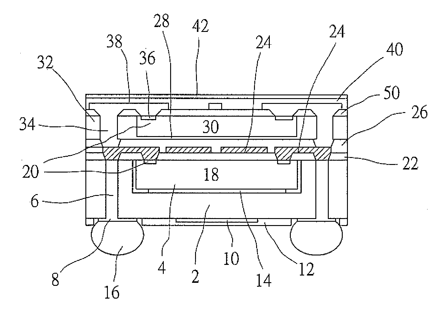
[0020]The present invention discloses a structure of WLP utilizing a substrate having predetermined circuit with through holes formed therein and a cavity formed into the substrate. A photosensitive material is coated over the die and the pre-formed substrate. Preferably, the material of the photosensitive material is formed of elastic material.

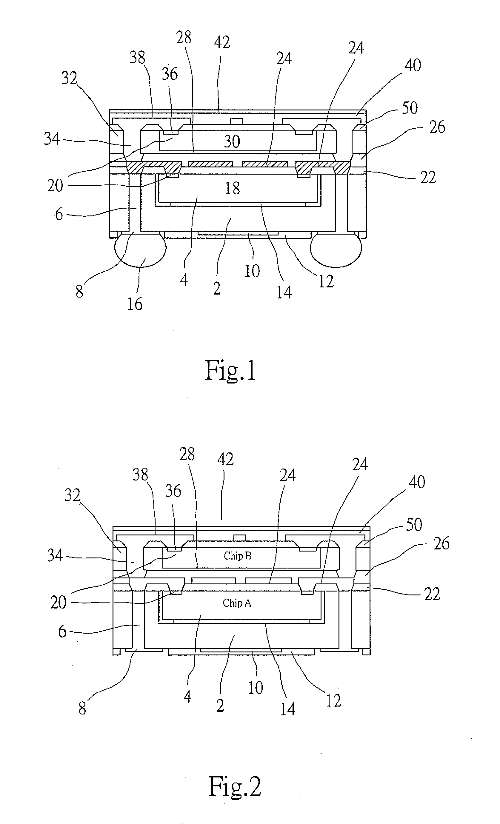
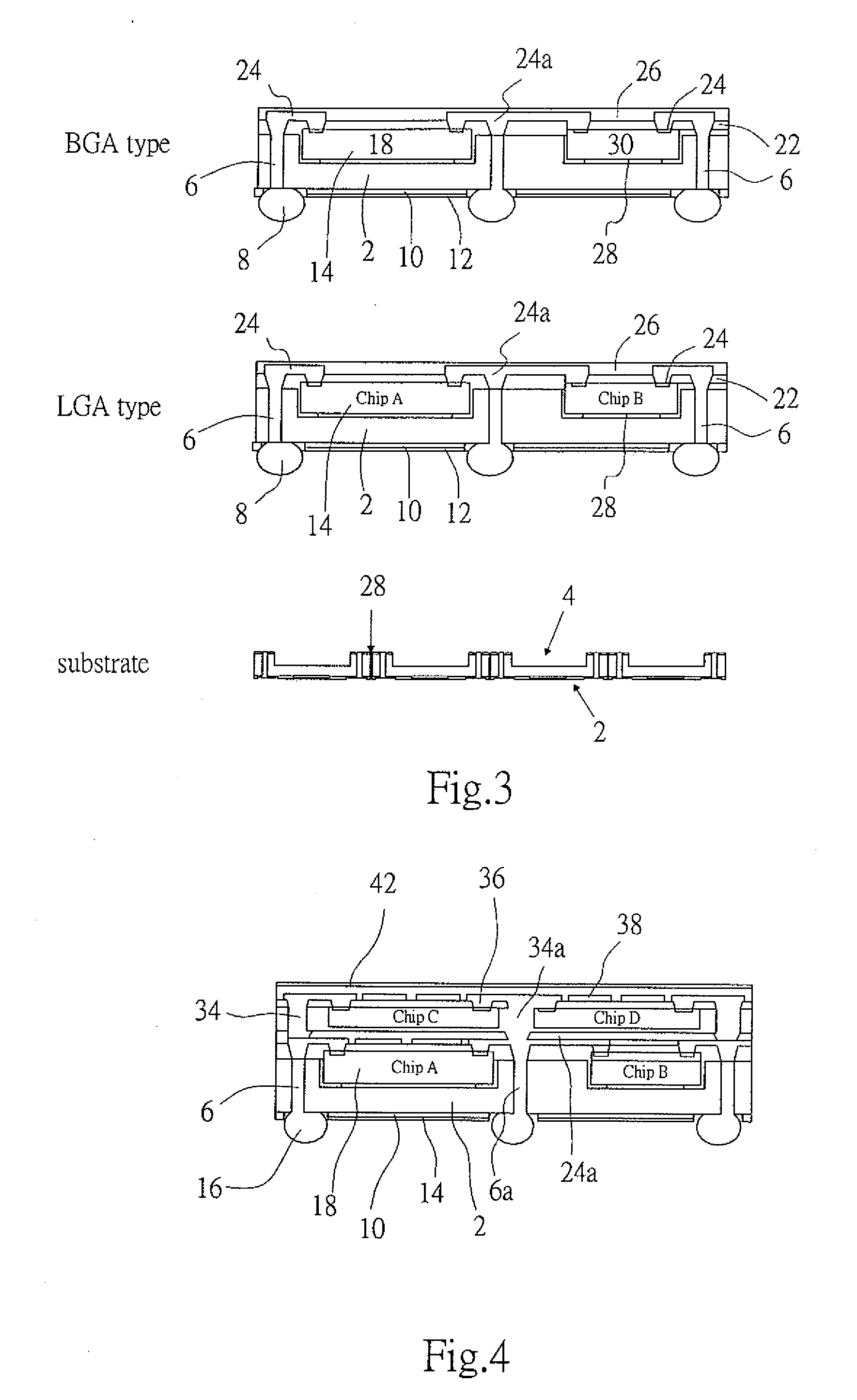
[0021]FIG. 1 illustrates a cross-sectional view of panel scale package (PSP) for SIP in accordance with one embodiment of the present inve...


PUM


Abstract

The present invention provides a structure of multi-chips package comprising: a substrate with a die receiving cavity formed within an upper surface of the substrate and a first through holes structure, wherein a terminal pads is formed under the first through holes structure. A first die is disposed within the die receiving cavity and a first dielectric layer is formed on the first die and the substrate. A first re-distribution conductive layer (RDL) is formed on the first dielectric layer. A second dielectric layer is formed over the first RDL and a second die is attached on the second dielectric layer. A surrounding material surrounds the second die. A third dielectric layer is formed over the second die and the surrounding material. A second re-distribution conductive layer (RDL) is formed on the third dielectric layer. A protection layer is formed over the second RDL.

Description

FIELD OF THE INVENTION[0001]This invention relates to a structure for system in Package (SIP), and more particularly to a panel scale package (PSP) with SIP.DESCRIPTION OF THE PRIOR ART[0002]In the field of semiconductor devices, the device density is increased and the device dimension is reduced, continuously. The demand for the packaging or interconnecting techniques in such high density devices is also increased to fit the situation mentioned above. Conventionally, in the flip-chip attachment method, an array of solder bumps is formed on the surface of the die. The formation of the solder bumps may be carried out by using a solder composite material through a solder mask for producing a desired pattern of solder bumps. The function of chip package includes power distribution, signal distribution, heat dissipation, protection and support. As a semiconductor become more complicated, the traditional package technique, for example lead frame package, flex package, rigid package techn...

Claims


Application Information

Patent Timeline
Patent Type & Authority Applications(United States)
IPC IPC(8): H01L23/02
CPCH01L24/82H01L2924/15153H01L25/0657H01L2225/06527H01L2225/06541H01L2924/01013H01L2924/01029H01L2924/01033H01L2924/01047H01L2924/01059H01L2924/01079H01L2924/01082H01L2924/09701H01L2924/15311H01L2924/01006H01L2924/01068H01L2924/01075H01L2924/01087H01L2924/014H01L2224/73267H01L2924/10253H01L25/0652H01L2224/92244H01L2224/04105H01L2224/24227H01L2224/32225H01L2924/00H01L2924/351H01L2924/14H01L2924/157H01L2924/15788H01L23/12H01L23/48
Inventor YANG, WEN-KUN
Owner ADVANCED CHIP ENG TECH
Why Eureka
Try Eureka