Transparent Planar Body and Transparent Touch Switch

Active Publication Date: 2008-06-12
GUNZE LTD
View PDF9 Cites 245 Cited by
  • Summary
  • Abstract
  • Description
  • Claims
  • Application Information

AI Technical Summary

Benefits of technology

[0047]The present invention provides a transparent planar bod

Problems solved by technology

In this structure, the shape of the pattern of the transparent electric conduction film that is f

Method used


Image

  • Transparent Planar Body and Transparent Touch Switch
  • Transparent Planar Body and Transparent Touch Switch
  • Transparent Planar Body and Transparent Touch Switch

Examples


first embodiment

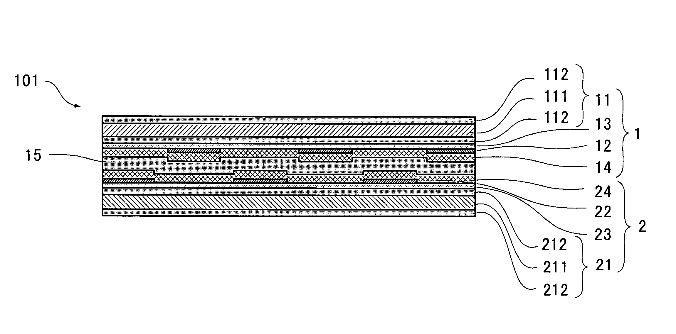
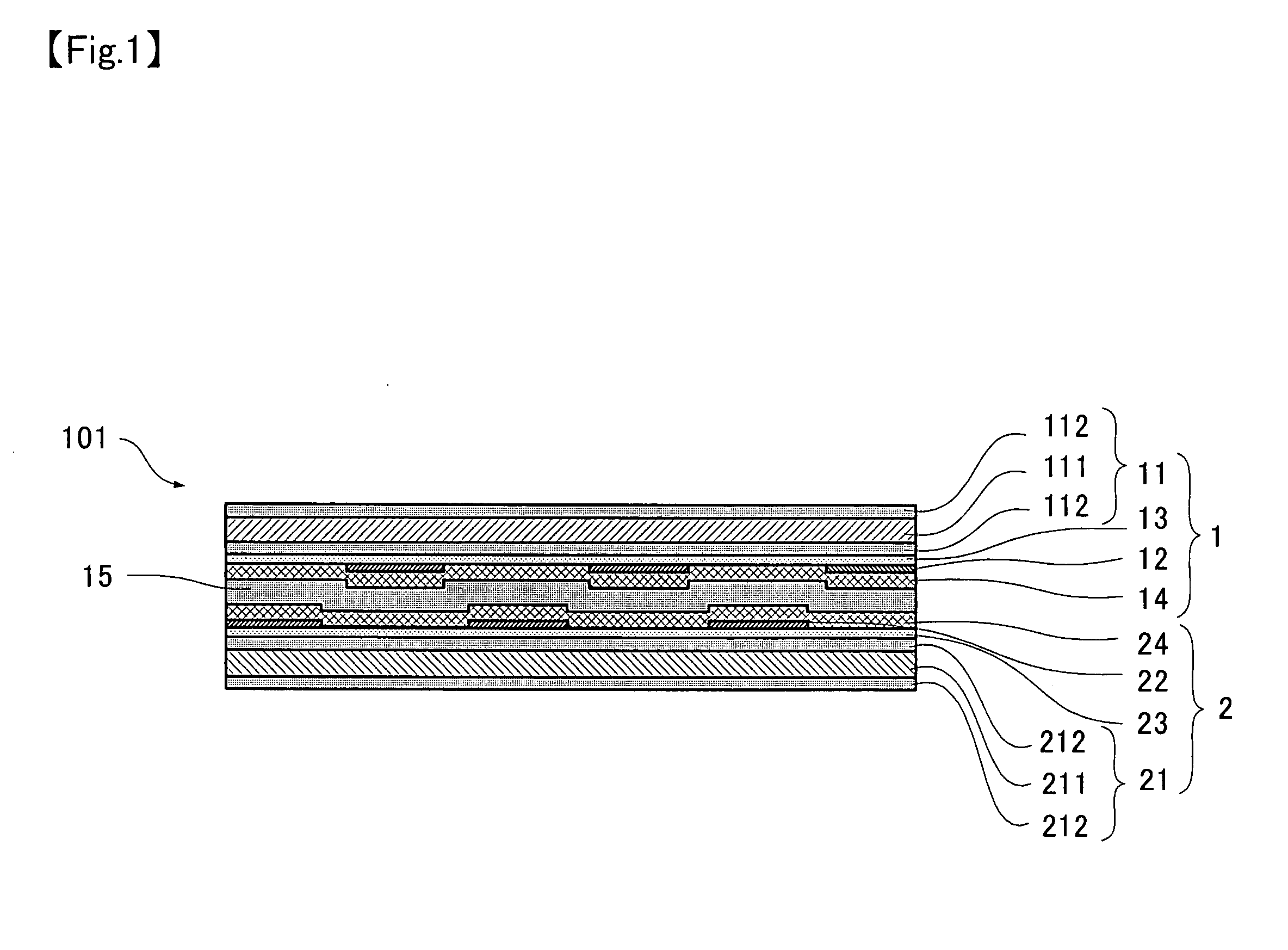
[0095]Hereunder, the first embodiment of the present invention are explained with reference to the drawings attached. To make the structure easier to understand, each component in the attached drawings is partially expanded or reduced and thus not shown to actual scale.

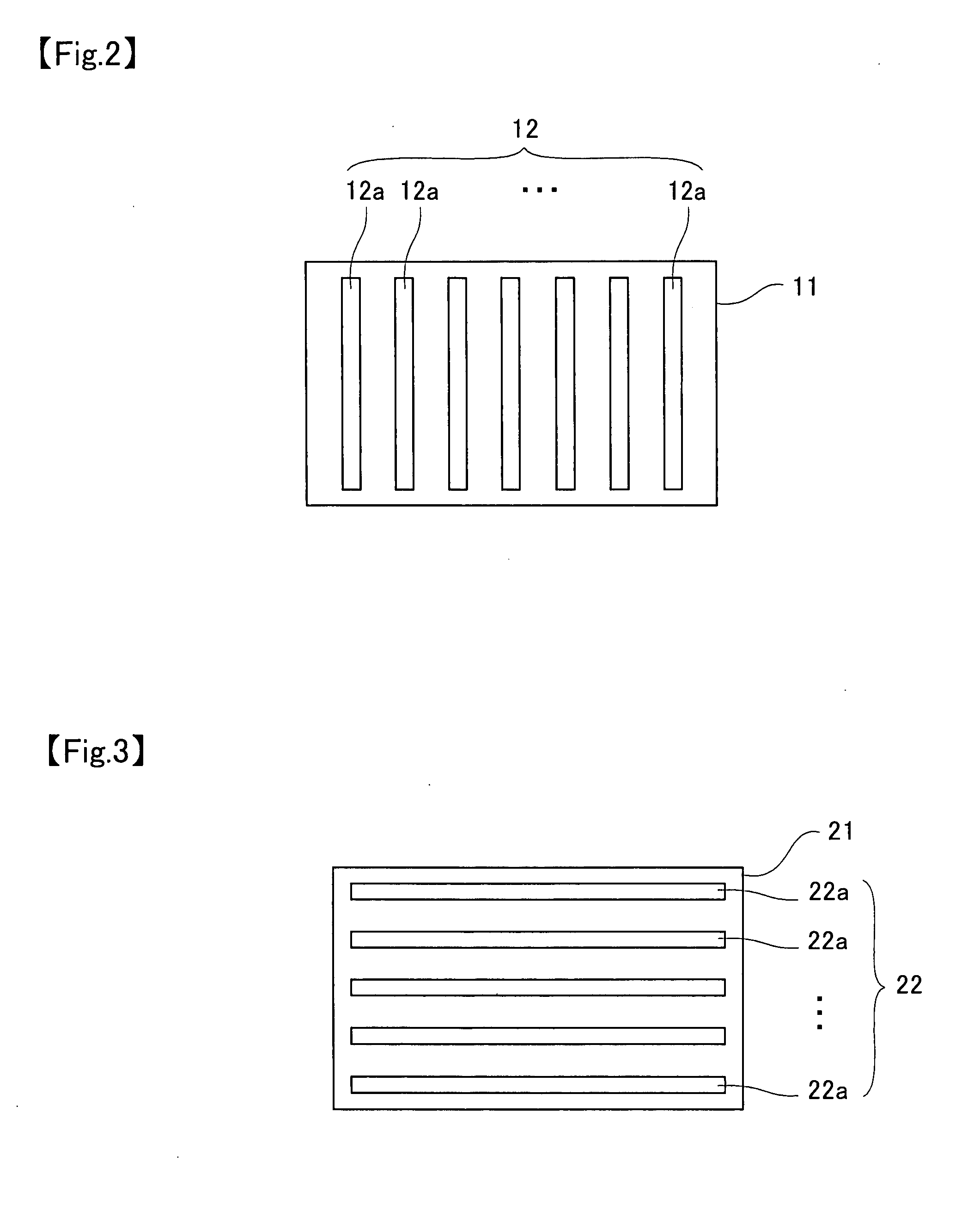
[0096]FIG. 1 is a schematic cross-sectional view showing the transparent touch switch of the first embodiment of the present invention. The transparent touch switch 101 is an electrostatic capacitive touch switch comprising a first transparent planar body 1 wherein a transparent conductive film 12 is formed on a transparent substrate 11 via an undercoat layer 13, and a second transparent planar body 2 wherein a transparent conductive film 22 is formed on a transparent substrate 21 via an undercoat layer 23. The first transparent planar body 1 and the second transparent planar body 2 are attached to each other via an adhesive layer 15 in such a manner that the transparent conductive films 12 and 22 face each other.

[009...

examples

[0115]The present invention is explained below based on Examples and Comparative Examples, but the scope of the invention is not limited to these Examples.

Example

[0116]Two measurement samples (5 cm×7 cm) as shown in FIGS. 6(a) and 6(b) were prepared to evaluate the difference in transmittance between the portions where a transparent conductive film 12 was provided and not provided in a transparent touch switch having the structure shown in FIG. 1. Sample A shown in FIG. 6(a) was a laminate wherein a transparent substrate 11, an undercoat layer 13, an overcoat layer 14, and an adhesive layer 15 are laminated in this order without providing a transparent conductive film. The transparent substrate 11 was formed in such a manner that two hard-coat layers 112 and 112 having a thickness of 3 to 5 μm was formed on the front and back surfaces of a base material layer 111 formed from a 200 μm thick PET film. The undercoat layer 13 was formed in such a manner that a silicon oxide layer having...

second embodiment

[0123]The second embodiment of the present invention is explained below with reference to the attached drawings. To make the structure easier to understand, each component in the attached drawings is partially expanded or reduced and thus not shown to actual scale.

[0124]FIG. 9 is a schematic cross-sectional view showing the transparent touch switch according to the second embodiment of the present invention. The transparent touch switch 101 is an electrostatic capacitive touch switch, which comprises a first transparent planar body 1 formed by providing a transparent conductive film 12 on a transparent substrate 11 via an undercoat layer 13; and a second transparent planar body 2 formed by providing a transparent conductive film 22 on a transparent substrate 21 via an undercoat layer 23. The first transparent planar body 1 and the second transparent planar body 2 are attached to each other via the adhesive layer 15 in such a manner that the transparent conductive films 12 and 22 fac...


PUM

PropertyMeasurementUnit
Thicknessaaaaaaaaaa
Thicknessaaaaaaaaaa
Thicknessaaaaaaaaaa

Abstract

The present invention provides a transparent planar body and a transparent touch switch that can improve visibility. Specifically, the transparent planar body (1) has a patterned transparent conductive film (12) on at least one surface of a transparent substrate (11). This transparent planar body (1) comprises a transmittance-adjusting layer for equalizing the transmission spectrum of light transmitted through a patterned region wherein the transparent conductive film (12) is provided via the transparent substrate (11) with that transmitted through a non-patterned region wherein the transparent conductive film (12) is not provided via the transparent substrate (11).

Description

TECHNICAL FIELD[0001]The present invention relates to a transparent planar body and a transparent touch switch.BACKGROUND OF THE INVENTION[0002]Various structures for transparent touch switches that can detect input position have been proposed such as a transparent electrostatic capacitive touch switch. For example, Patent Document 1 discloses a transparent touch switch comprising a dielectric layer lying between a pair of transparent planar bodies each provided with a transparent conductive film patterned into a predetermined shape. When an operator touches the operation surface with a finger, etc., the transparent touch switch detects the touched position by sensing the change of electric capacity via grounding through a human body.[0003]Such a transparent touch switch is mounted on the surface of a liquid crystal display apparatus, CRT or the like. In this structure, the shape of the pattern of the transparent electric conduction film that is formed in the transparent planar body...

Claims


Application Information

Patent Timeline
IPC IPC(8): G06F3/044G06F3/041H01B5/14
CPCG06F3/044Y10T428/24802G06F3/045G06F3/041H01H13/83G06F3/0446G06F3/0445G06F3/0412H01B5/14G06F2203/04103G06F3/0448H03K17/962H03K17/9645
Inventor WAKABAYASHI, NAOHIROYAMADA, TSUTOMUSASAKI, KUNIAKIFURUKAWA, SHUJITSUKAMOTO, KEIJI
Owner GUNZE LTD
Why Eureka
Try Eureka