
Self-timing read architecture for semiconductor memory and method for providing the same

a read architecture and read technology, applied in the direction of information storage, static storage, digital storage, etc., can solve the problem of small statistical deviation between the predetermined voltage created on the bit line and the arrival of the ‘sense-on’ signal, and achieve the effect of minimizing resistance differences

Inactive Publication Date: 2008-06-19
STMICROELECTRONICS PVT LTD
View PDF2 Cites 0 Cited by
  • Summary
  • Abstract
  • Description
  • Claims
  • Application Information

AI Technical Summary

Benefits of technology

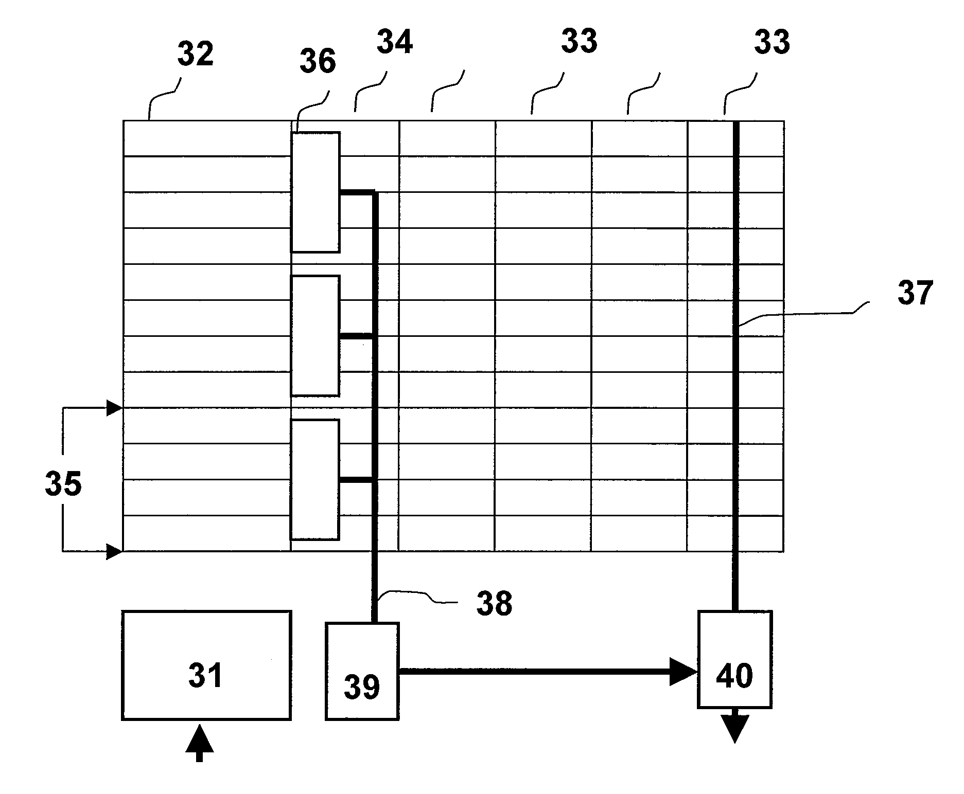
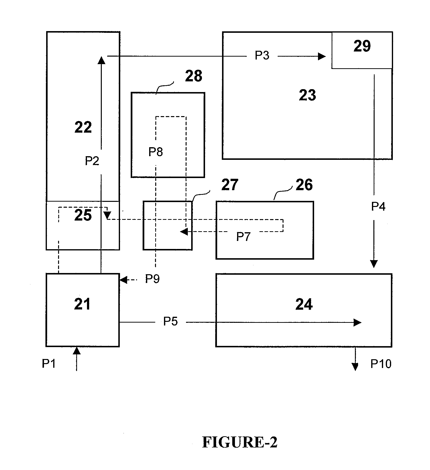
"The present disclosure is about a semiconductor memory device with a self-timing circuit that provides stability against operating conditions and ensures high speed and robustness. The device includes a control circuit, decoder circuit, timing circuit, output circuit, and memory region. The memory region is divided into clusters of memory cells, with each cluster including a dummy cell that has the same electrical characteristics as the memory cells in the cluster. The dummy cells are in close physical proximity to the memory cells and the first bit line to minimize differences in resistance. The device also includes an activation circuit to determine a discharge voltage on the dummy cell and a sensing circuit to read data from the memory cells in each cluster. The technical effects of the invention include high speed and robustness of the memory device, as well as control over the read access time and the ability to adjust the number of dummy cells in a particular cluster to control the time delay between accessing a normal memory cell and reading the data stored in the accessed memory cell."

Problems solved by technology

Moreover, the statistical deviation between the predetermined voltage created on the bit line and the arrival of the ‘sense-on’ signal is also very small.

Method used


Image

  • Self-timing read architecture for semiconductor memory and method for providing the same
  • Self-timing read architecture for semiconductor memory and method for providing the same
  • Self-timing read architecture for semiconductor memory and method for providing the same

Examples


Embodiment Construction

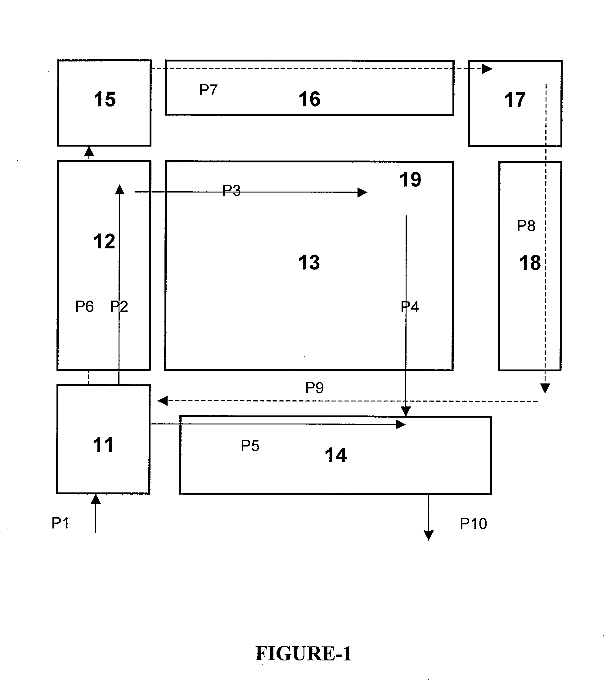
[0027]FIG. 1 shows the block diagram of a semiconductor memory device presently used. The device includes a control circuit 11, a decoder circuit 12, a memory cell array 13, a read write amplifier 14, a dummy word decoder 15, a dummy word line 16, a dummy memory cell 17, and a dummy bit line 18. During a read operation, the decoder circuit 12 selectively activates a word line of a memory cell array 13 when a clock signal and an address signal are supplied to the control circuit 11 from an exterior of the device. The decoder circuit supplies a read signal to a memory cell 19. The read signal propagates along the path P1, P2, P3. Data read from the memory cell 19 is then supplied to the read—write amplifier through a path P4. In parallel the dummy word decoder 15 activates the dummy word line 16 based on a clock signal CK, and the address signal ADDRESS supplied to the control circuit 11 from the exterior of the device, thereby supplying a read signal to the dummy memory cell 17. The ...


PUM


Abstract

A semiconductor memory device having a control circuit, decoder circuit, a dummy column, and a normal memory cell array divided in clusters of N consecutive rows, where N can be one or more than one, and for each cluster of N rows a common circuitry is used in block with a dummy bit line connected to the dummy column and to a timing circuit. A normal bit line connected to the normal memory cells provides the read normal bit to input / output logic. Whenever a normal memory cell is accessed during the read operation, the circuitry of the corresponding dummy row enables the dummy bit line to discharge, and when the voltage across the dummy bit line reaches a predetermined value, the timing circuit produces a timing signal to activate the input / output circuitry to read the data stored in the accessed memory cell.

Description

BACKGROUND OF THE INVENTION[0001]1. Field of Invention[0002]The present invention relates to self-timing read architecture for a semiconductor memory device.[0003]2. Description of the Related Art[0004]A semiconductor memory is composed of data storage cells arranged in rows and columns. The process of reading from the memory is accomplished by means of control, address and input / output signals. At the time of reading, a set of external control signals and a clock are activated. The memory cell from which the data is to be read is accessed and then the data is read by the read circuitry connected between the output data lines of the memory.[0005]The read circuitry performs the reading operation by sensing the voltage difference developed across the data lines. However, in order to ensure that desired data is read correctly, the read operation should be performed only when a sufficient voltage differential has been developed across the data lines. This is done by ensuring a predeterm...

Claims


Application Information

Patent Timeline
Patent Type & Authority Applications(United States)
IPC IPC(8): G11C7/06
CPCG11C7/08G11C7/227G11C7/22
Inventor AHMAD, NASIM
Owner STMICROELECTRONICS PVT LTD
Learn More