Process for integratng a iii-n type component on a (001) nominal silicium substrate

Inactive Publication Date: 2008-06-26
STMICROELECTRONICS SRL
View PDF3 Cites 15 Cited by
  • Summary
  • Abstract
  • Description
  • Claims
  • Application Information

AI Technical Summary

Benefits of technology

[0022]It is another object of the present invention to provide an alternate to the known technique for growing GaN on off-oriented silicon, so as to remedy the drawbacks to such techniques, and allow integration of GaN on a substrate which is fully compatible with known MOS/C

Problems solved by technology

The former substrate has a low thermal conductivity thus limiting its use for power applications, while the latter substrate shows higher conductivity but at a significantly high manufacturing cost.
This technique allows mass production of discrete GaN components but unfortunately does not allow the integration of such components in the traditional silicon wafer used for the integration of the usual MOS/CMOS type components, since that integration is based on a (001) orientation of the silicon substrate.
As a consequence, there is no possibility of real integration with MOS/CMOS microelectronics circuits and (1,1,1) oriented silicon substrates can only serve as a suppor

Method used


Image

  • Process for integratng a iii-n type component on a (001) nominal silicium substrate
  • Process for integratng a iii-n type component on a (001) nominal silicium substrate
  • Process for integratng a iii-n type component on a (001) nominal silicium substrate

Examples


second embodiment

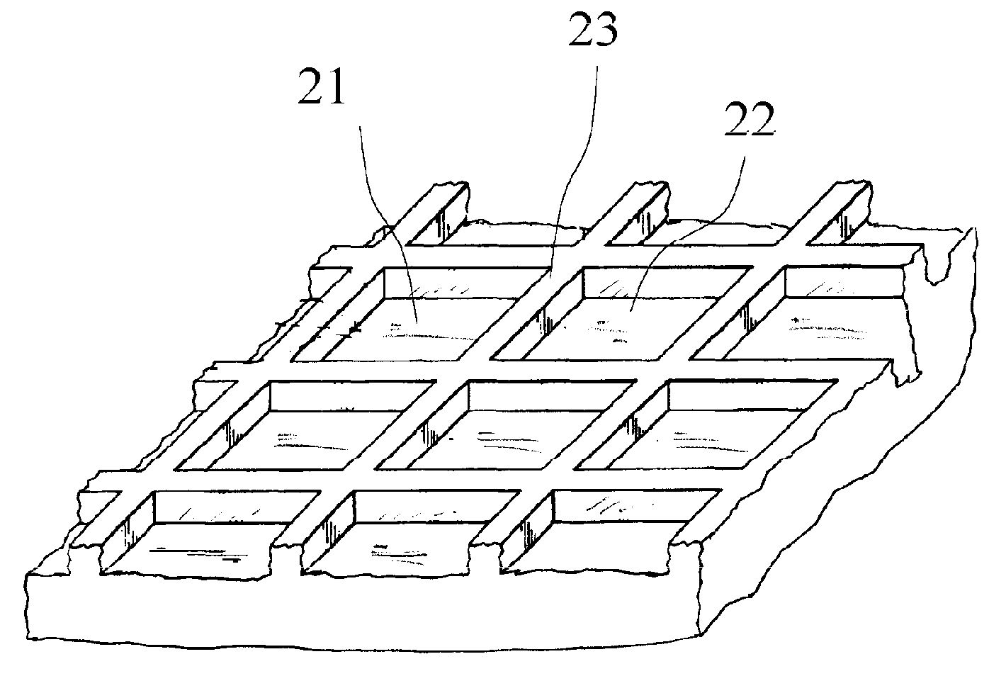
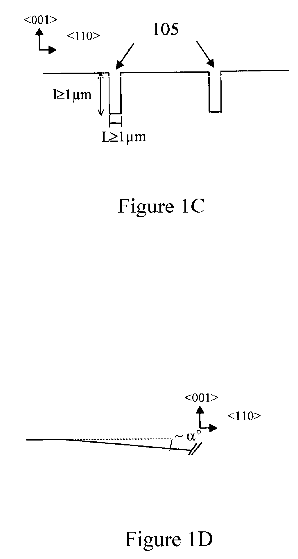
[0042]In a second embodiment, the hosting area takes the form of a hollow or an engraved area, preferably having a dimension within the range [10×10, 10×100].

third embodiment

[0043]In a third embodiment, the substrate comprises several hosting areas located in the same plane and separated from each other by a trench.

fourth embodiment

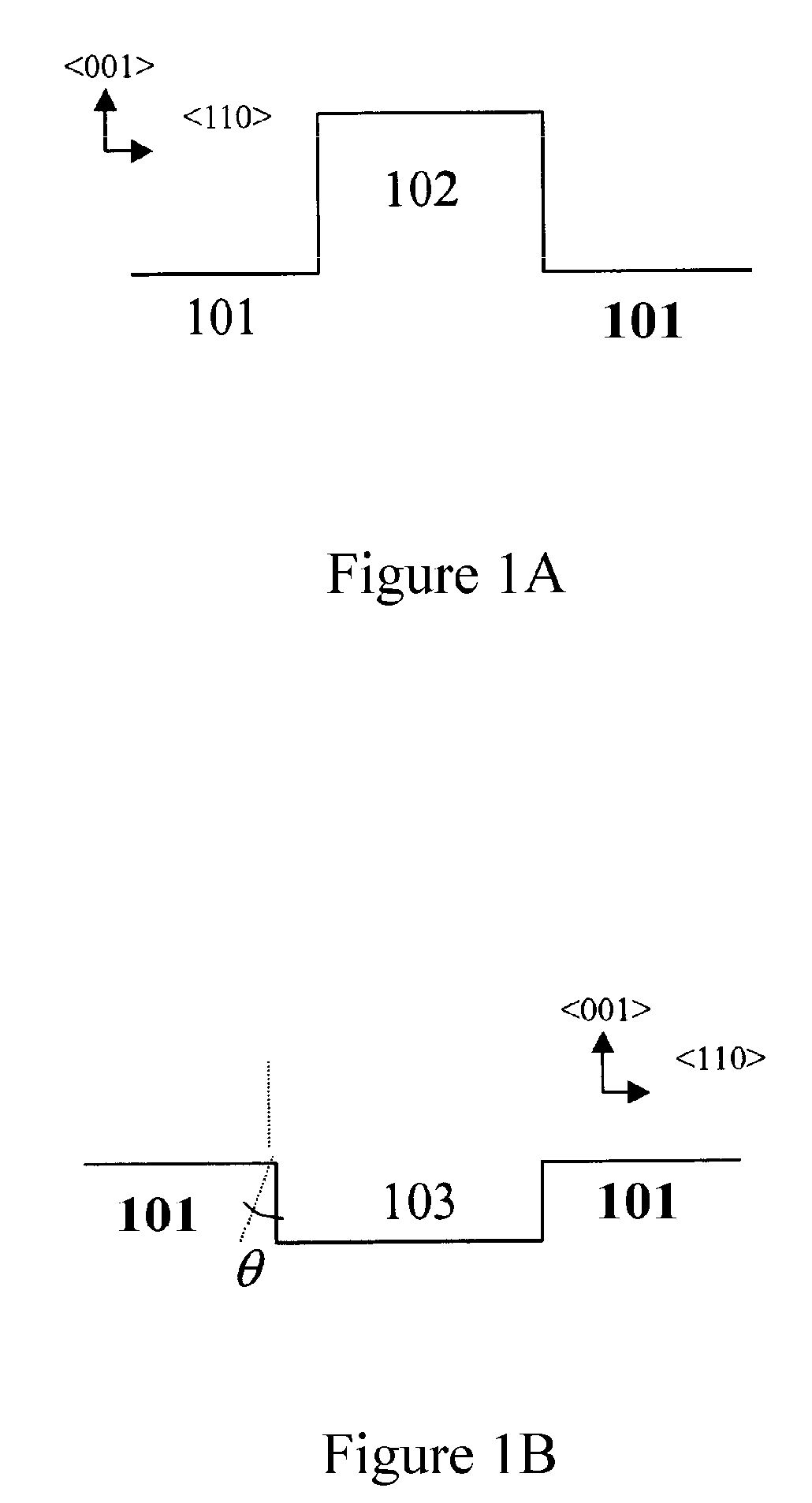
[0044]In a fourth embodiment, the hosting area shows a local off-orientation resulting in bi-atomic steps.

[0045]Preferably, the III-V component is a GaN component.

[0046]The present invention also provides a semiconductor device based on a (001) or (100) nominal substrate. According to a preferred embodiment, the device includes a texture made of elementary areas each comprising an elementary surface, with the texture comprising at least one hosting area which is locally prepared so as to present one single privileged type of terrace, and with each hosting area comprising at least one AlN layer and a layer of III-V component forming an hetero-structure. The device also includes a MOS / CMOS structure (or others) on non-hosting areas.

[0047]In one embodiment, the hosting areas have been processed by high temperature vacuum heating or, alternatively, by a stabilization phase of the bi-atomic steps.

[0048]The hosting area preferably takes the form of a square or rectangular area having a si...


PUM


Abstract

A process is provided for integrating a III-N component, such as GaN, on a (001) or (100) nominal silicon substrate. There are arranged a texture of elementary areas each comprising an individual surface, with the texture comprising at least one hosting area intended to receive a III-N component. A mask layer is deposited on non-hosting areas which are not intended to receive a III-N type component. The hosting area is locally prepared so as to generate on the surface of the area one domain comprising one single type of terrace. There is grown by Molecular Beam Epitaxy or Metalorganic Vapor Phase Epitaxy on the hosting area one intermediary AlN buffer layer, followed by the growth of one III-N based material so as to realize a substantially monocrystalline structure. There is eliminated the mask layer located on non-hosting areas as well as surface polycrystalline layers deposited above the mask layers, and MOS/CMOS structures are subsequent integrated on at least some of the non-hosting areas.

Description

CROSS-REFERENCE TO RELATED APPLICATIONS[0001]This application is based upon and claims priority from French Patent Application No. 06 10040, filed Nov. 17, 2006, the entire disclosure of which is herein incorporated by reference.FIELD OF THE INVENTION[0002]The present invention relates to processes for manufacturing microelectronic circuits, and more particularly to a process for integrating a III-N type component, such as GaN, on a (001) nominal silicon substrate.BACKGROUND OF THE INVENTION[0003]GaN based components are booming because of the increasing interest in opto-electronic circuits, and more particularly in electro-luminescent and laser diodes which are spreading on the market.[0004]Elsewhere there can also be noticed a significant development of power electronic circuits, in which GaN components are likely to have large part, particularly with the development of AlGaN / GaN High Electron Mobility Transistors (H.E.M.T.)[0005]In the past, the first components which were based ...

Claims


Application Information

Patent Timeline
IPC IPC(8): H01L21/763H01L31/0368
CPCC30B23/025C30B23/04C30B25/04C30B25/183C30B29/406H01L21/02381H01L33/007H01L21/0254H01L21/02639H01L21/02658H01L21/02664H01L27/0605H01L29/2003H01L21/02458
Inventor JOBLOT, SYLVAINSEMOND, FABRICEMASSIES, JEANCORDIER, YVONDUBOZ, JEAN-YVES
Owner STMICROELECTRONICS SRL
Why Eureka
Try Eureka