Light emission diode

Active Publication Date: 2008-06-26
LEXTAR ELECTRONICS CORP
View PDF1 Cites 27 Cited by
  • Summary
  • Abstract
  • Description
  • Claims
  • Application Information

AI Technical Summary

Benefits of technology

[0008]The primary purpose of the present invention is to provide an improved construction of a light emitting diode to correct t

Problems solved by technology

Nonetheless, the frame 11 is related to a straight and flushed structure and when the plastic casing 14 is formed on the area of two carriers 111, the positioning effect by contact between the plastic casing and the frame 11 is comprised of two straight and flushed contact planes resulting in poor positioning effect

Method used


Image

  • Light emission diode
  • Light emission diode
  • Light emission diode

Examples


Embodiment Construction

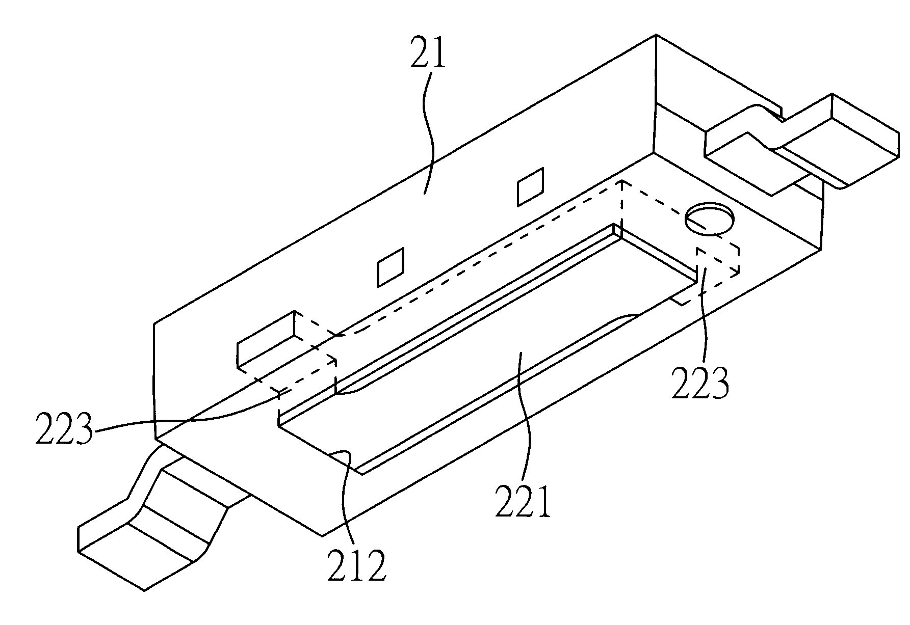
[0021]Referring to FIGS. 3, 4, and 5 for a preferred embodiment of the present invention, a light emitting diode 2 includes a casing 21 containing a frame 22; and the casing is provided with an accommodation recess 211 to expose the frame 22.

[0022]The frame 22 is provided with a placement area 221 to receive placement of a light-emitting chip 23, and an electrode area 222 separating from the placement area 221. A sectional fall area 223 is disposed at where appropriately on the placement area 221. As illustrated, the sectional fall 223 is disposed at the bottom of the placement area 221. A protruding portion 224 extends from one side of the placement area 221 so that the side of the placement area becomes a non-flushed structure. The electrode area 222 is comprised of one or a plurality of pair of positive and negative electrode areas 2221, 2222 that are separated from each other by polarity.

[0023]One or a plurality of light emitting chip 23 is placed on the placement area 221 and e...


PUM


Abstract

A light emitting diode includes a casing, a frame in the casing, one or a plurality of light emitting chip, and a packaging polymer; the frame being provided with a placement area to receive placement of the light emitting chip, and an electrode area separated from the placement area; a sectional fall being disposed at where appropriately on the placement area to increase contact area between the frame and the casing and improve the relative stability between the casing and the frame.

Description

BACKGROUND OF THE INVENTION[0001](a) Field of the Invention[0002]The present invention is related to a light emission diode (LED), and more particularly, to one that is capable of helping secure the casing in relation to the frame and improving heat sink effect.[0003](b) Description of the Prior Art[0004]Whereas a light emitting diode is related to a light emitting device comprised of semi-conductor that produces spectra of different frequency by emitting photons as a result of having the electrons incorporated with electric holes in the semiconductor crystal; that is, when a light emission chip of integrated n-type semiconductor crystal and p-type semiconductor crystal is conducted, extra electronics from the n-type semiconductor crystal will flow into the electric holes in the p-type semiconductor crystal; and energy is released when electronics from the n-type conductor crystal flow into electric holes in the p-type semiconductor crystal due to difference in potentials. The energ...

Claims


Application Information

Patent Timeline
IPC IPC(8): F21V15/01H01L33/48H01L33/62H01L33/64
CPCH01L25/0753H01L33/486H01L33/62H01L33/642H01L33/647H01L2924/01322H01L2224/48247H01L2224/48257H01L2224/48091H01L2924/00014
Inventor SU, WEN-LUNGHSIEH, HSIANG-CHENG
Owner LEXTAR ELECTRONICS CORP
Why Eureka
Try Eureka