Nonvolatile nanotube diodes and nonvolatile nanotube blocks and systems using same and methods of making same

a technology of nonvolatile nanotube blocks and nanotube diodes, applied in nanoinformatics, instruments, basic electric elements, etc., can solve the problem of limited application to otp memories, and achieve the effect of low resistance state and high resistance sta

Active Publication Date: 2008-07-03
NANTERO
View PDF96 Cites 78 Cited by
  • Summary
  • Abstract
  • Description
  • Claims
  • Application Information

AI Technical Summary

Benefits of technology

[0040]Under another aspect, a two-terminal non-volatile state device includes: first and second terminals; a semiconductor field effect element having a source, a drain, a gate in electrical communication with one of the source and the drain, and a channel disposed between the source and the drain, the gate capable of controllably forming an electrically conductive pathway in the channel between the source and the drain; a nanotube switching element having a nanotube fabric article and a conductive contact, the nanotube fabric article disposed between and capable of forming an electrically conductive pathway between the conductive contact and the second terminal; wherein the first terminal is in electrical communication with one of the source and the drain, the other of the source and drain is in electrical communication with the conductive contact; and wherein a first set of electrical stimuli on the first and second conductive terminals causes a first logic state and a second set of electrical stimuli on the first and second conductive terminals causes a second logic state.
[0041]One or more embodiments include one or more of the following features. The first logic state corresponds to a relatively non-conductive pathway between the first and second terminals and the second logic state corresponds to a conduc...

Problems solved by technology

These required larger memories at increasingly higher densities, sold in increasing volumes, and at lower cost per bit, are challenging the semiconductor industry to rapidly improve geometries and process features.
The storage cell is large because of large polysilicon fuse dimensions, so the OTP memory described in U.S...

Method used


Image

  • Nonvolatile nanotube diodes and nonvolatile nanotube blocks and systems using same and methods of making same
  • Nonvolatile nanotube diodes and nonvolatile nanotube blocks and systems using same and methods of making same
  • Nonvolatile nanotube diodes and nonvolatile nanotube blocks and systems using same and methods of making same

Examples


Embodiment Construction

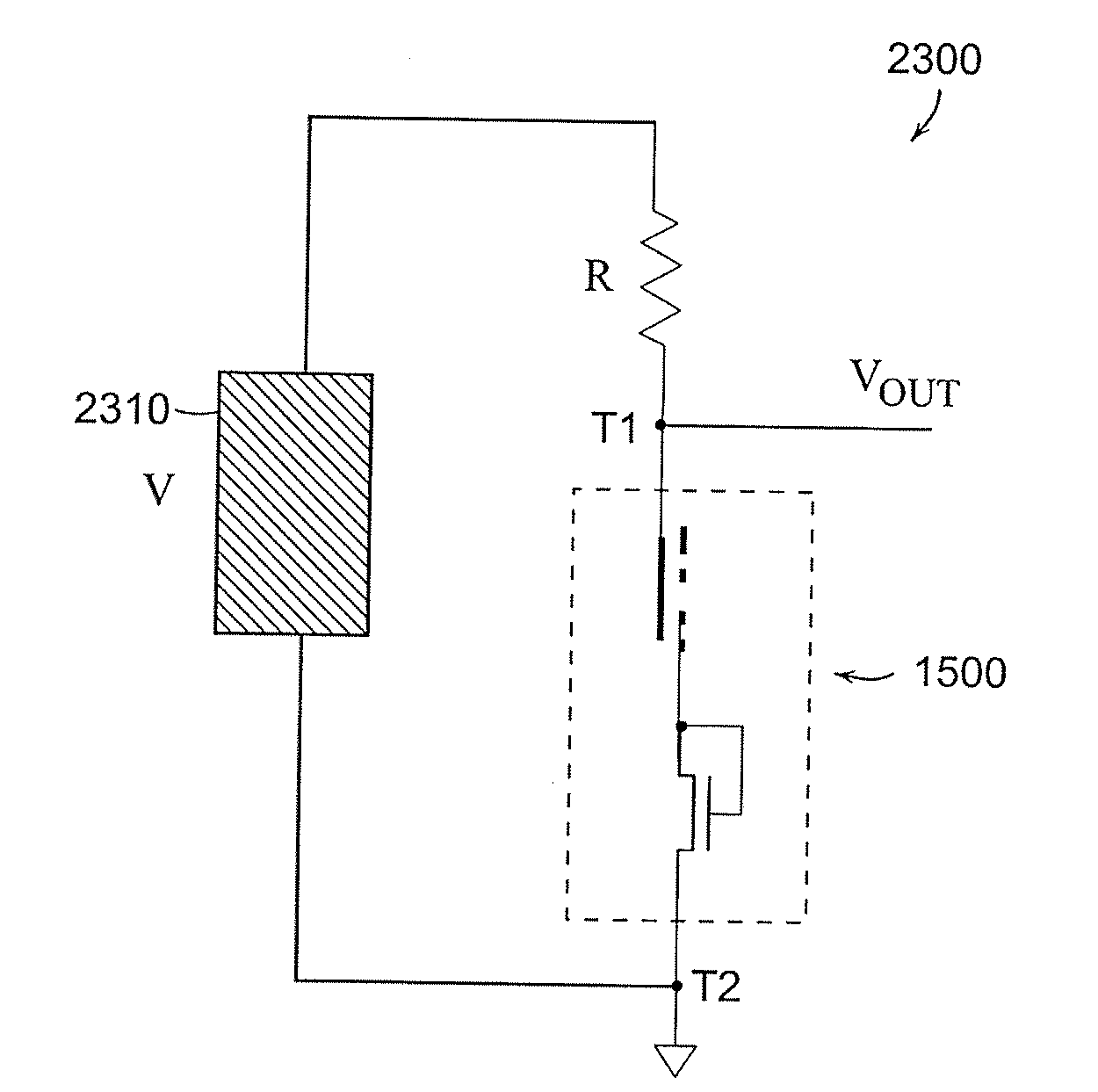
[0151]Embodiments of the present invention provide nonvolatile diodes and nonvolatile nanotube blocks and systems using same and methods of making same.

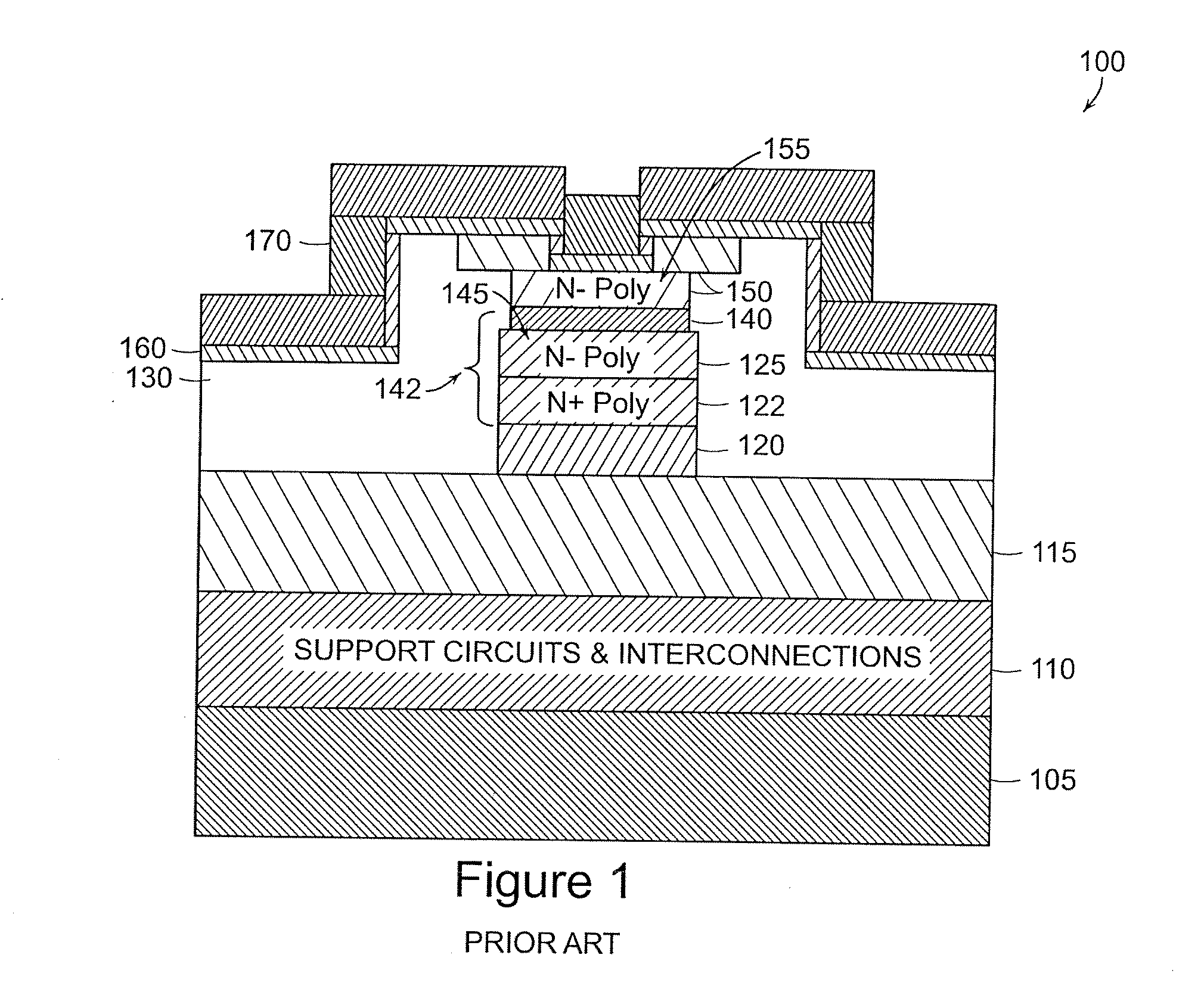
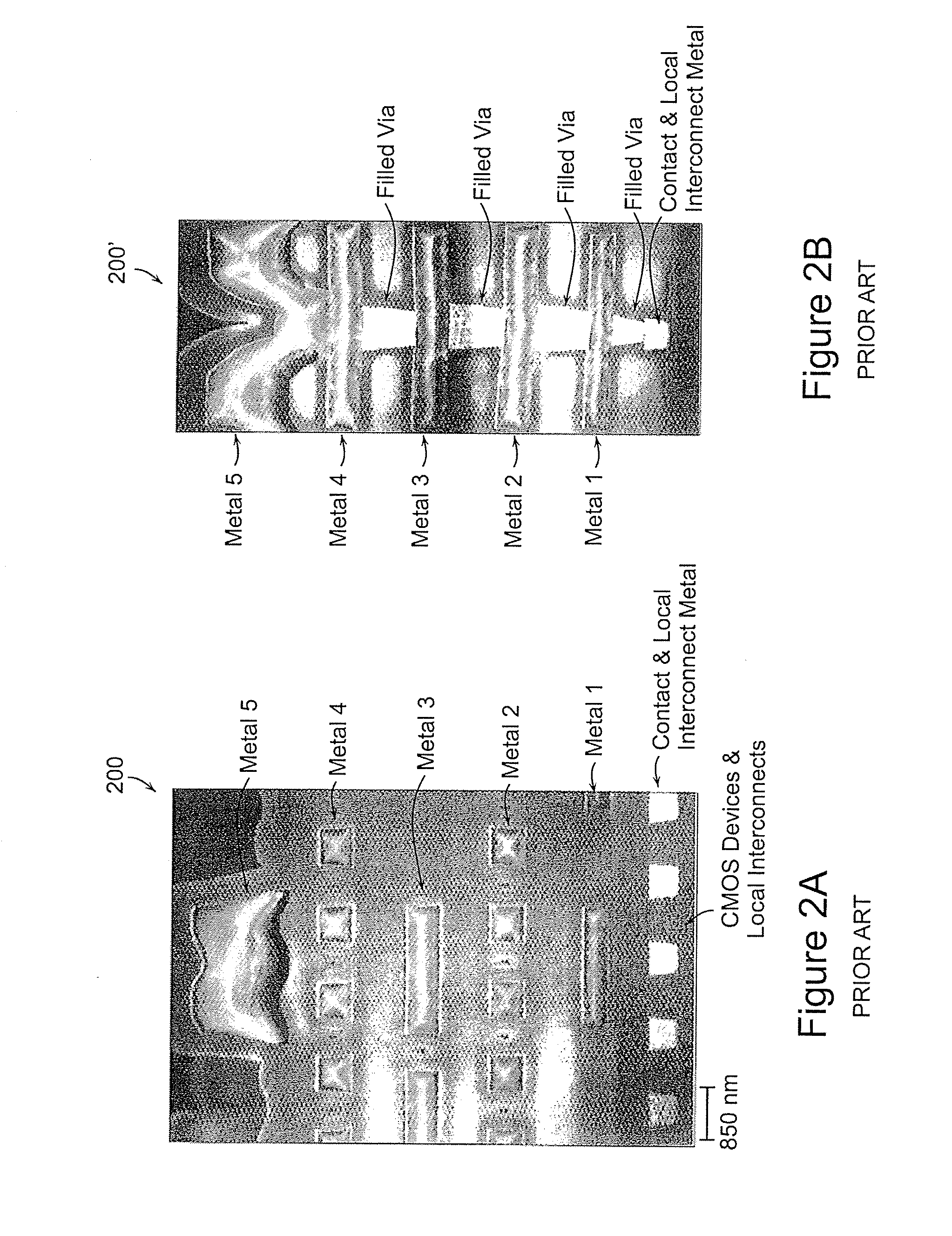
[0152]Some embodiments of the present invention provide 3-D cell structures that enable dense nonvolatile memory arrays that include nanotube switches and diodes, can write logic 1 and 0 states for multiple cycles, and are integrated on a single semiconductor (or other) substrate. It should be noted that such nonvolatile memory arrays may also be configured as NAND and NOR arrays in PLA, FPGA, and PLD configurations for performing stand-alone and embedded logic functions as well.

[0153]Some embodiments of the present invention provide diode devices having nonvolatile behavior as a result of diodes combined with nonvolatile nanotube components, and methods of forming such devices.

[0154]Some embodiments of the present invention also provide nanotube-based nonvolatile random access memories that include nonvolatile nanotube diode device ...


PUM


Abstract

Under one aspect, a nanotube diode includes: a cathode formed of a semiconductor material; and an anode formed of nanotubes. The cathode and anode are in fixed and direct physical contact, and are constructed and arranged such that sufficient electrical stimulus applied to the cathode and the anode creates a conductive pathway between the cathode and the anode. In some embodiments, the anode includes a non-woven nanotube fabric having a plurality of unaligned nanotubes. The non-woven nanotube fabric may have a thickness, e.g., of 0.5 to 20 nm. Or, the non-woven nanotube fabric may include a block of nanotubes. The nanotubes may include metallic nanotubes and semiconducting nanotubes, and the cathode may include an n-type semiconductor material. A Schottky barrier can form between the n-type semiconductor material and the metallic nanotubes and/or a PN junction can form between the n-type semiconductor material and the semiconducting nanotubes.

Description

CROSS REFERENCE TO RELATED APPLICATIONS[0001]This application claims the benefit under 35 U.S.C. § 119(e) of the following applications, the entire contents of which are incorporated herein by reference:[0002]U.S. Provisional Patent Application No. 60 / 855,109, entitled “Nonvolatile Nanotube Blocks,” filed on Oct. 27, 2006;[0003]U.S. Provisional Patent Application No. 60 / 840,586, entitled “Nonvolatile Nanotube Diode,” filed on Aug. 28, 2006;[0004]U.S. Provisional Patent Application No. 60 / 836,437, entitled “Nonvolatile Nanotube Diode,” filed on Aug. 8, 2006;[0005]U.S. Provisional Patent Application No. 60 / 836,343, entitled “Scalable Nonvolatile Nanotube Switches as Electronic Fuse Replacement Elements,” filed on Aug. 8, 2006; and[0006]U.S. Provisional Patent Application No. 60 / 918,388, entitled “Memory Elements and Cross Point Switches and Arrays of Same Using Nonvolatile Nanotube Blocks,” filed on Mar. 16, 2007.[0007]This application is a continuation-in-part of and claims priority ...

Claims


Application Information

Patent Timeline
IPC IPC(8): H01L29/06
CPCB82Y10/00G11C13/025G11C2213/19H01L21/8221H01L23/5256H01L27/0688H01L2924/0002H01L27/1021H01L27/1203H01L2924/00
Inventor BERTIN, CLAUDE L.RUECKES, THOMASHUANG, X. M. H.SIVARAJAN, RAMESHGHENCIU, ELIODOR G.KONSEK, STEVEN L.MEINHOLD, MITCHELL
Owner NANTERO
Why Eureka
Try Eureka