Nonvolatile memory device using a threshold voltage switching material and method for manufacturing same

a switching material and non-volatile technology, applied in the field of memory devices, can solve the problems of low power consumption efficiency, data retention capability lowering, operation speed degrading, etc., and achieve the effect of improving reliability and fast programming

Active Publication Date: 2014-02-06
KOREA UNIV RES & BUSINESS FOUND
View PDF1 Cites 2 Cited by
  • Summary
  • Abstract
  • Description
  • Claims
  • Application Information

AI Technical Summary

Benefits of technology

[0025]Accordingly, the nonvolatile memory device of the present invention does not use tunneling during programming and changes the resistance state of the threshold voltage switching material into a low resistance state in order to perform a program operation. Also, in order to maintain the charges trapped in the charge trap layer, no additional voltage pulse is required for converting the resistance state of the threshold voltage switching material into the high resistance state again. Therefore, fast

Problems solved by technology

However, as the nonvolatile memory device becomes small and integrated, a data retention capability is lowered due to leakage current, and power consumption efficiency is low due to a high operation voltage.
Firstly, in a case where a tunneling insulation layer formed of a silicon oxide film of a single layer has a reduced thickness for an enhanced operation speed, it cannot obtain a data retention characteristic more than 10 years, a characteristic of a nonvolatile memory, due to increase of direct tunneling and stress induced leakage current. If the thickness of the silicon oxide film is increased, a data retention characteristic more than 10 years can be obtained. However, in this case, an operation speed may be degraded, and a high voltage may be required.
Secondly, when performing an erasing operation using a b

Method used


Image

  • Nonvolatile memory device using a threshold voltage switching material and method for manufacturing same
  • Nonvolatile memory device using a threshold voltage switching material and method for manufacturing same
  • Nonvolatile memory device using a threshold voltage switching material and method for manufacturing same

Examples


Embodiment Construction

[0031]Hereinafter, preferred embodiments of the present invention will be explained with reference to the attached drawings.

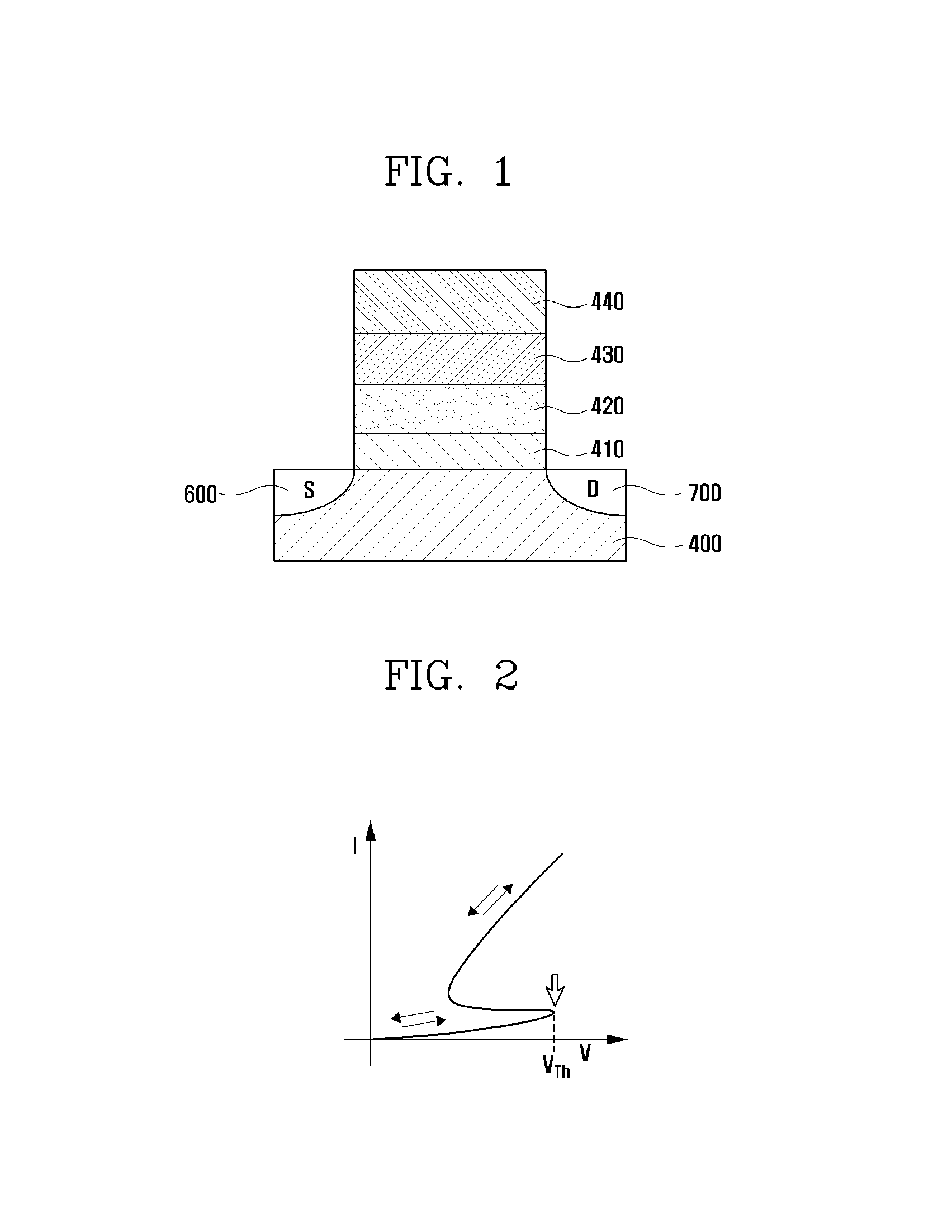
[0032]FIG. 1 is a view showing a structure of a nonvolatile memory device according to a preferred embodiment of the present invention.

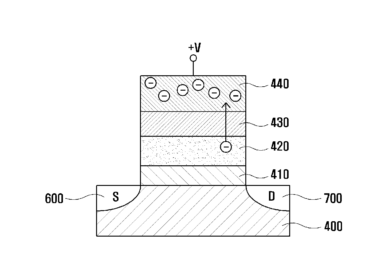
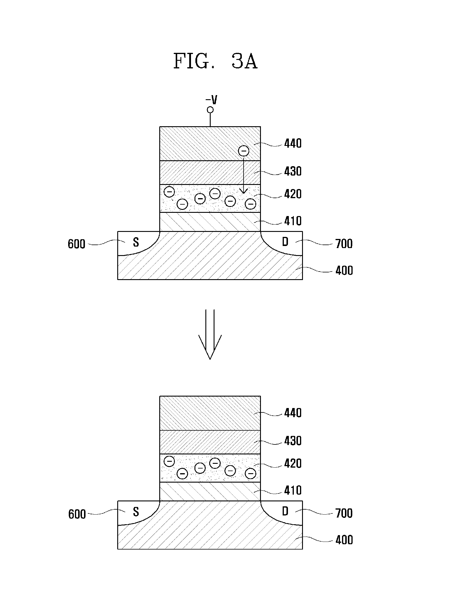
[0033]Referring to FIG. 1, the nonvolatile memory device according to the present invention has a structure where a memory layer is formed on a semiconductor substrate 400, and a source region 600 and a drain region 700 are formed on the semiconductor substrate 400 at both sides of the memory layer.

[0034]The memory layer formed on the semiconductor layer 400 includes a first insulation layer 410 formed on the semiconductor layer 400, a charge trap layer 420 formed on the first insulation layer 410, a second insulation layer 430 formed on the charge trap layer 420, and a gate electrode layer 440 formed on the second insulation layer 430.

[0035]The first insulation layer 410 prevents charges trapped in the charge trap layer 420, fr...


PUM


Abstract

The present invention relates to a nonvolatile memory device and to a method for manufacturing same. According to the present invention, the blocking insulation layer of a nonvolatile memory device having a typical SONOS structure is replaced with a threshold voltage switching material, which changes to a low resistance state only while a voltage greater than a threshold voltage is applied while maintaining a high resistance state under normal conditions and returning to the high resistance state when the applied voltage is removed. The present invention performs a program operation by injecting charges from a gate electrode layer into a charge trap layer through an insulation layer formed of the threshold voltage switching material after applying a voltage pulse greater than the threshold voltage to the gate electrode layer.

Description

TECHNICAL FIELD[0001]The present invention relates to a memory device and a method for manufacturing the same, and more particularly, to a nonvolatile memory device and a method for manufacturing the same.BACKGROUND ART[0002]Recently, as demand for portable information devices such as smart phones drastically increases, required is developing a nano-sized nonvolatile memory (NVM) device capable of implementing ultra large scale integration (terabit), an ultra-miniaturized size, a high speed and high reliability.[0003]However, as the nonvolatile memory device becomes small and integrated, a data retention capability is lowered due to leakage current, and power consumption efficiency is low due to a high operation voltage.[0004]Accordingly, has been proposed a polySilicon-Oxide-Nitride-Oxide-Silicon (SONOS) type memory device having a memory characteristic of a high performance and compatible with the conventional processes, as the next generation nonvolatile memory device. However, s...

Claims


Application Information

Patent Timeline
IPC IPC(8): H01L29/792G11C11/34H01L29/66
CPCH01L29/792G11C11/34H01L29/66833H01L29/42332H01L29/66825H01L29/7881G11C13/0002
Inventor KIM, TAEGEUNAN, HOMYOUNG
Owner KOREA UNIV RES & BUSINESS FOUND
Why Eureka
Try Eureka