Phase change memory array with integrated polycrystalline diodes

a technology of phase change memory array and polycrystalline diodes, which is applied in the field of semiconductor devices and processing, can solve problems such as device-to-device non-uniformity in the on characteristics of diodes, and achieve the effect of high resistive sta

Active Publication Date: 2019-04-09
IBM CORP
View PDF9 Cites 3 Cited by
  • Summary
  • Abstract
  • Description
  • Claims
  • Application Information

AI Technical Summary

Benefits of technology

[0006]Yet another method for deactivating memory cells affected by the presence of grain boundaries in polycrystalline selection devices includes forming one or more amorphous material layers on a metal layer; crystallizing at least one of the one or more amorphous material layers to form polycrystalline material in a diode stack; facilitating dopant diffusion across grain boundaries of the polycrystalline material to create shunts across the grain boundaries; forming phase change memory material within the diode stack; forming a second contact layer on the diode stack; patterning the diode stack and the phase change memory material to form selection diodes and phase change memory elements connected between metal lines in a crossbar array; annealing to achieve a crystalline state in the phase change memory elements; identifying memory cells having shunted diodes by scanning the array using smaller negative sense voltages; and applying larger negative voltages to the phase change memory elements gated by the shunted selection diodes such that the phase change memory elements gated by the shunted diodes achieve a permanently high resistive state.

Problems solved by technology

However, given that a diode is a minority carrier device, its OFF characteristics may be more sensitive to grain boundary dislocations than a majority carrier device such as a field effect transistor.
In addition, the presence of grain boundaries may induce device-to-device non-uniformity in the ON characteristics of the diode.

Method used


Image

  • Phase change memory array with integrated polycrystalline diodes
  • Phase change memory array with integrated polycrystalline diodes
  • Phase change memory array with integrated polycrystalline diodes

Examples


Embodiment Construction

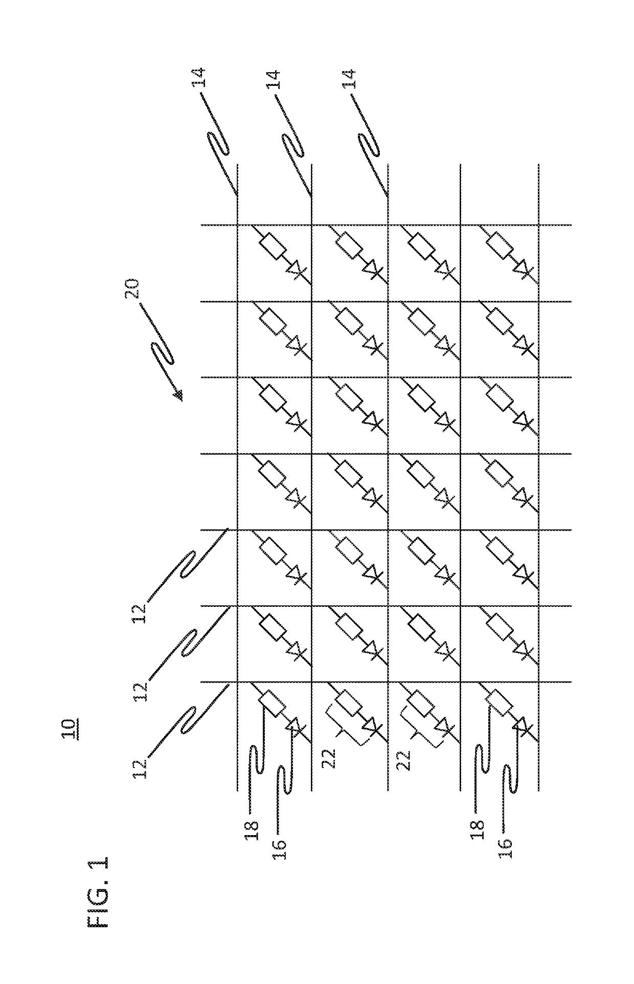
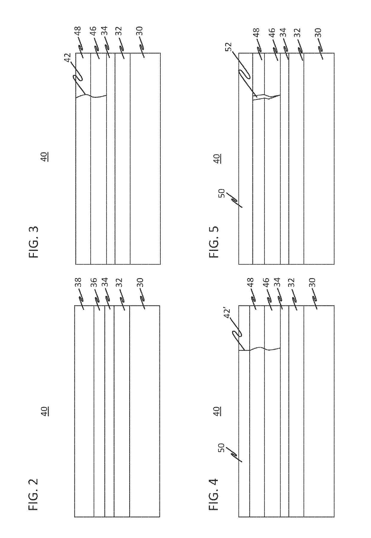
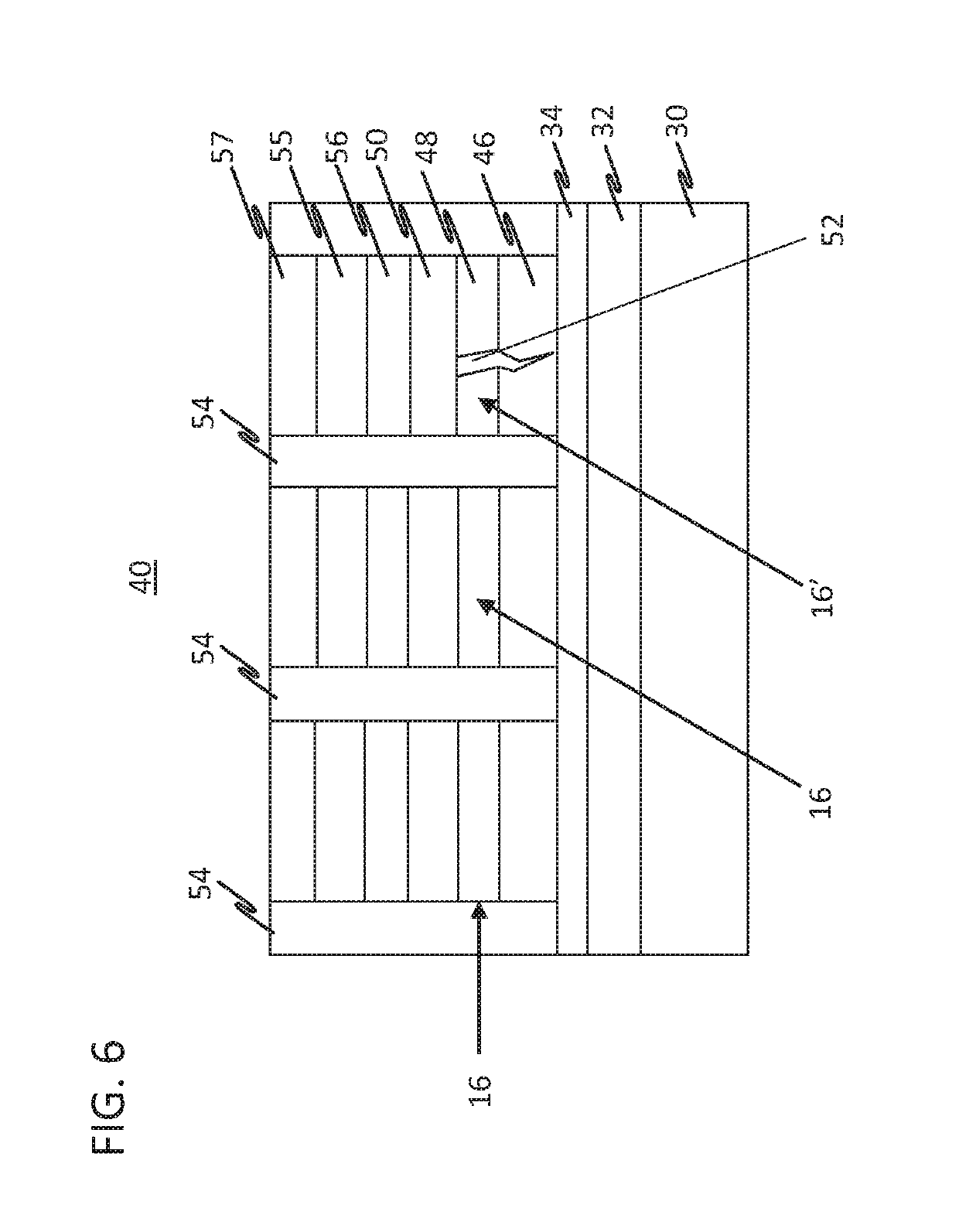
[0023]In accordance with aspects of the present invention, structures and methods are provided that can employ diodes as selection devices. Selection devices can include a switch or configuration that permits selection of a path or state. In the present example, selection devices will be described in terms of access devices for memory cells. In particularly useful embodiments, selection devices can include diodes employed with phase change memory structures to function as memory cells. In accordance with aspects of the present invention, low-temperature polysilicon (poly-Si) (LTPS) prepared by excimer laser anneal (ELA) is a candidate for integrating diode selection devices with a phase-change memory (PCM) array. The diode has the potential to program multi-level memory cells. The PCM array with integrated LTPS-based selection diodes may be fabricated in back-end-of-line (BEOL).

[0024]To enable the advantages of polycrystalline diodes as selection devices, the adverse effects associa...


PUM


Abstract

A method for deactivating memory cells affected by the presence of grain boundaries in polycrystalline selection devices includes crystallizing a semiconductor layer in a diode stack to form a polycrystalline layer for selection diodes formed in a crossbar array. To achieve a crystalline state in phase change memory elements coupled to corresponding selection diodes perform an anneal. Memory cells having shunted selection diodes due to grain boundaries are identified by scanning the array using sense voltages. A second voltage larger than the sense voltages is applied to the phase change memory elements gated by the shunted selection diodes such that the phase change memory elements gated by the shunted diodes achieve a permanently high resistive state.

Description

BACKGROUNDTechnical Field[0001]The present invention generally relates to semiconductor devices and processing, and more particularly to structures and methods that enable selective removal of memory cells affected by the presence of the grain boundaries.Description of the Related Art[0002]A diode has a simple structure, a small footprint and is capable of providing high drive currents. Compared to an Ovonic Threshold Switch (OTS), a diode benefits from established device physics / fabrication technology, better reliability, and high-temperature stability. However, given that a diode is a minority carrier device, its OFF characteristics may be more sensitive to grain boundary dislocations than a majority carrier device such as a field effect transistor. In addition, the presence of grain boundaries may induce device-to-device non-uniformity in the ON characteristics of the diode.SUMMARY[0003]In accordance with an embodiment of the present invention, a method for deactivating memory ce...

Claims


Application Information

Patent Timeline
Patent Type & Authority Patents(United States)
IPC IPC(8): H01L27/24G11C13/00H01L45/00H01L21/02
CPCH01L27/2409H01L21/02532H01L21/02381G11C13/0004H01L45/06H01L45/1616H01L27/2463H01L21/0262G11C2213/72H01L21/02576H01L21/02579H10B63/20H10B63/80H10N70/231H10N70/8828H10N70/063H10N70/023
Inventor HEKMATSHOARTABARI, BAHMANLAM, CHUNG H.CARTA, FABIOBRIGHTSKY, MATTHEW J.
Owner IBM CORP
Why Eureka
Try Eureka