

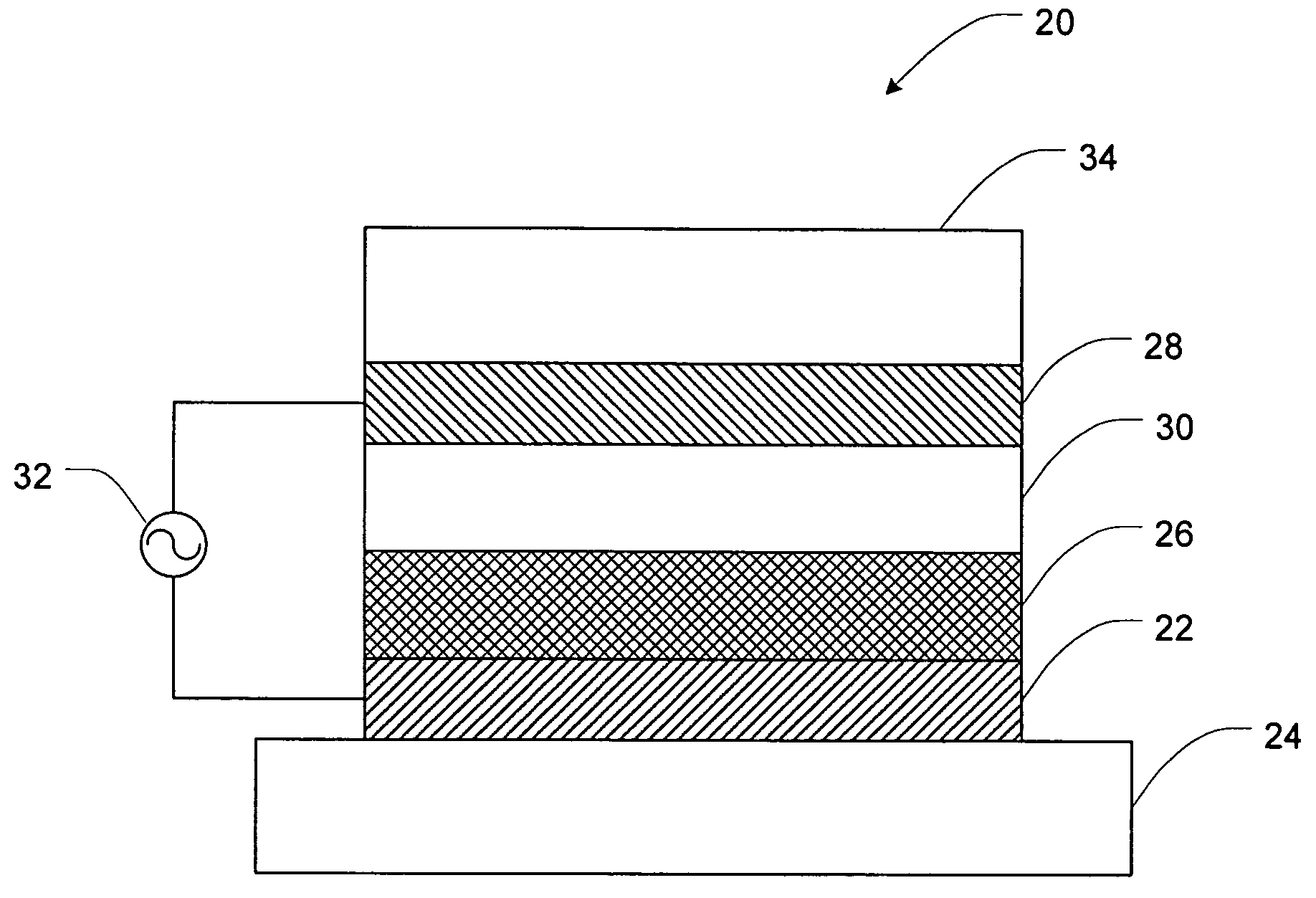
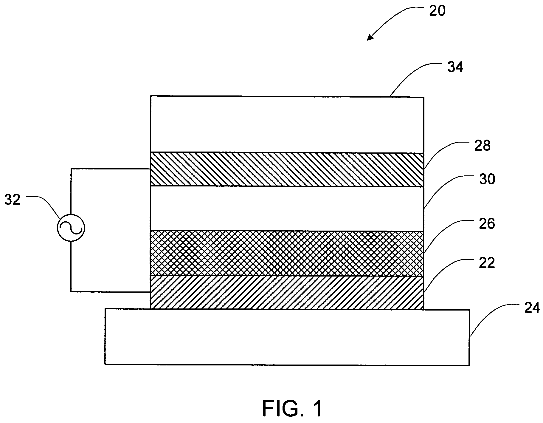
Printing conductive patterns using LEP
a technology of conductive patterns and printed circuits, applied in the direction of conductors, instruments, semiconductor/solid-state device details, etc., can solve the problems of reducing the performance of fabricated devices, losing the shape accuracy of electronic devices or integrated circuits being created, and expensive and slow processing
- Summary
- Abstract
- Description
- Claims
- Application Information
AI Technical Summary
Benefits of technology
Problems solved by technology
Method used
Image

Examples
example 1
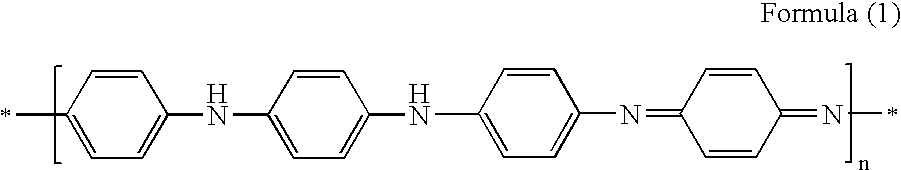
[0043]Emeraldine base based ElectroInk is made as follows: 30-50 wt % by solids of emeraldine base is mixed with resin F varnish. Resin F varnish is a copolymer of polyacrylic acid and polyethylene. The two components are ground in S-0 atritor (made by Union process, Akron, Ohio USA) for about 4 hours in 19 wt % non volatile solid (NVS). The resulting slurry is diluted to 2 wt %. A solution of 5 wt % aluminum di / tri butoxide (ALB) is added to give 0.5 wt % of ALB by solids. The diluted slurry mixture is mixed for approximately 5 minutes. A 0.3 wt % amount of NCD (charge director) is added to give 50-70 pMoh (Moh=1 / Ohm) low field conductivity. The particle conductivity of the resulting emeraldine base ink can be measured to be in the range of 150-200 pMoh.
example 2
[0044]A conductive pattern can be created as follows: The 2 wt % emeraldine base ink is printed in a pattern on a paper substrate using an LEP process. In this case an Ultra-Stream LEP printer can be used. The pattern is allowed to dry in air and later heat fused on a hot plate to give an insulating pattern. The insulating pattern is covered with a 10 wt % solution of sulfuric acid for 5 minutes. The product of the emeraldine base and the sulfuric acid results in an emeraldine salt. The acid solution is wiped off the substrate. The print resolution is about 100 μm. The conductivity of the pattern can be measured to be about 15 kΩ by two probe measurement.
example 3
[0045]A conductive additive can be included as follows: A carrier resin (varnish) of 40 wt % NVS is ground with the combination of carbon black (Vulcan XC72) and the formulation of emeraldine base from Example 1 to total 60 wt % NVS. The resultant formulation is printed with a LEP process onto paper to give films with different conductivities based on the amount of carbon black in the formulation. The conductivity of the conductive pattern increases as the % carbon black in the formulation is increased.
PUM
| Property | Measurement | Unit |
|---|---|---|
| resistance | aaaaa | aaaaa |
| resistance | aaaaa | aaaaa |
| wt % | aaaaa | aaaaa |
Abstract
Description
Claims
Application Information