

Heat dissipation semiconductor pakage
a technology of semiconductor pakage and heat dissipation, which is applied in the direction of semiconductor devices, semiconductor/solid-state device details, electrical apparatus, etc., can solve the problems of wasting substrate space, affecting the electried performance and product stability of the semiconductor chip, and the dissipation structure itself being not able to be mounted, so as to achieve the effect of dissipating hea
- Summary
- Abstract
- Description
- Claims
- Application Information
AI Technical Summary
Benefits of technology
Problems solved by technology
Method used
Image

Examples
first embodiment
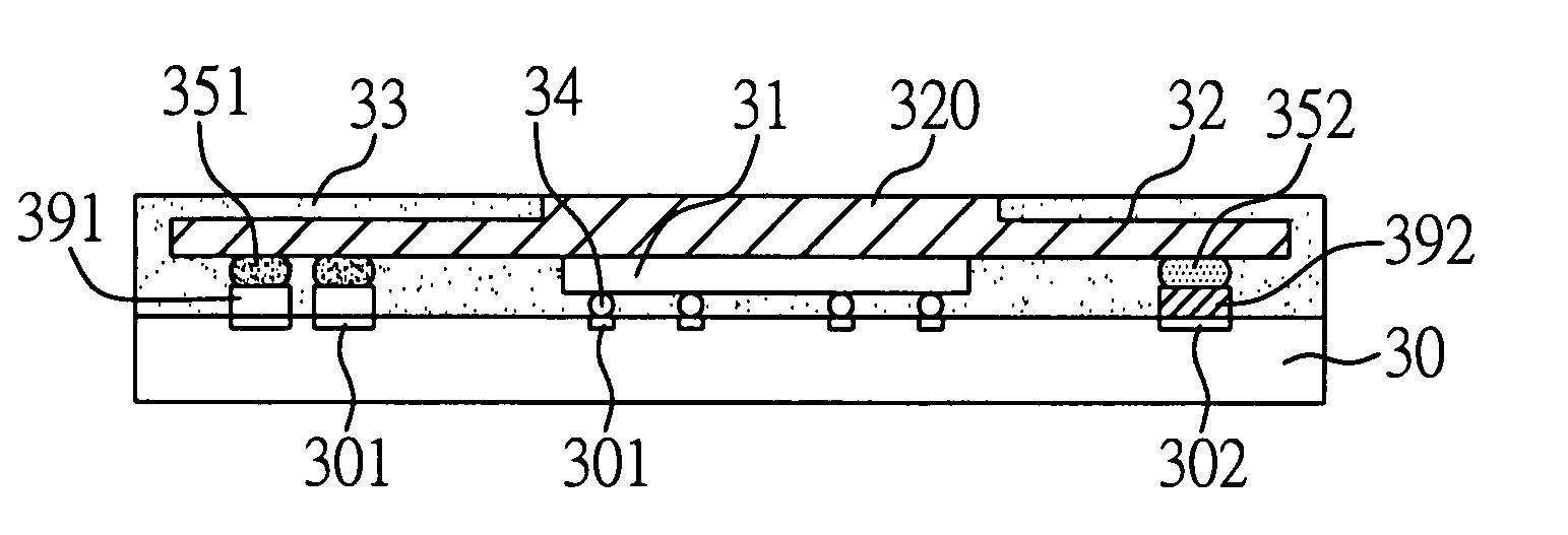
[0030]Please refer to FIGS. 3A and 3B, which are diagrams of planar view and section view of the first embodiment of a heat dissipation semiconductor package according to the present invention.
[0031]As shown in the figures, the heat dissipation semiconductor package comprises: a substrate 30, which has a plurality of solder pads 301 and at least a ground pad 302 set on a surface thereof; at least a semiconductor chip 31, which is mounted on the substrate 30 and electrically connects to the solder pads 301; a plurality of passive elements 391, which are mounted on and electrically connect to the solder pads 301 of the substrate 30; at least a passive element of zero resistance 392, which is mounted on and electrically connects to the ground pad 302; and a heat sink 32, which is mounted on the passive elements 391, and electrically connects to the passive element of zero resistance 392.
[0032]The substrate 30 can be, for example, a ball grid array substrate, and a surface of the substr...
second embodiment
[0041]Please refer to FIGS. 4A through 4C, which are diagrams of the second embodiment of a heat dissipation semiconductor package according to the present invention, wherein, FIG. 4B is a section view diagram corresponding to the heat dissipation semiconductor package of FIG. 4A.
[0042]The heat dissipation semiconductor package disclosed in the second embodiment of the present invention is applicable to situations such as: when regular passive elements can not be used as support structures, or to prevent the regular passive elements from being damaged, in the present embodiment, a plurality of ground pads 302 are formed on around corners or along margins of the substrate 30 (as shown in FIGS. 4A and 4B), and have at least three passive elements of zero resistance or metal bumps 38 be mounted on and electrically connect to the ground pads 302, meanwhile set a plurality of solder pads 301 on other area of the substrate 30 for mounting and electrically connecting to a semiconductor chi...
third embodiment
[0043]Please refer to FIG. 5, which is a diagram of the third embodiment of a heat dissipation semiconductor package of the present invention, the heat dissipation semiconductor package of the present embodiment is mostly similar to the ones of the foregoing embodiments, the main difference is that the heat sink 32 of the present invention can further be mounted on the semiconductor chip 31 via thermal grease 37, thereby helping to dissipate heat generated due to semiconductor chip operation.
PUM
 Abstract
Description
Claims
Application Information