Method and structure for fabricating solar cells using a layer transfer process

a layer transfer and solar cell technology, applied in semiconductor/solid-state device manufacturing, electrical equipment, semiconductor devices, etc., can solve the problems of not possessing the optimum properties of highly effective solar cells, many limitations of solar cells, and difficult manufacturing of materials, etc., to achieve high-quality photovoltaic power, efficient technique for large-scale manufacturing, and high-quality photovoltaic

Inactive Publication Date: 2008-07-03
SILICON GENERAL CORPORATION
View PDF9 Cites 117 Cited by
  • Summary
  • Abstract
  • Description
  • Claims
  • Application Information

AI Technical Summary

Benefits of technology

[0014]Numerous benefits may be achieved over pre-existing techniques using the present invention. In particular, embodiments in accordance with the present invention use controlled energy and selected conditions to preferentially cleave a thin photovoltaic film onto a glass substrate according to a specific embodiment. In a specific embodiment, the present method and device provides a very high quality photovoltaic material on glass, which can be used as a portion of the packaging material. In a preferred

Problems solved by technology

Unfortunately, such petroleum sources have become depleted and have lead to other problems.
Although effective, these solar cells still have many limitations.
These materials are often difficult to manufacture.
Although these plates may be formed effectively, they do not possess optimum properties for highly effective solar cells.
Such single crystal silic

Method used


Image

  • Method and structure for fabricating solar cells using a layer transfer process
  • Method and structure for fabricating solar cells using a layer transfer process
  • Method and structure for fabricating solar cells using a layer transfer process

Examples


Embodiment Construction

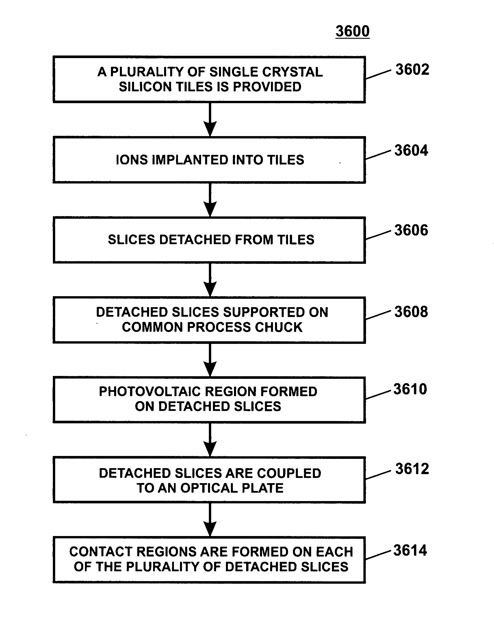
[0037]According to embodiments of the present invention, techniques directed to the manufacture of photovoltaic materials are provided. More particularly, embodiments of the present invention provide a technique including a method and a structure for forming a solar cell structure using layer transfer techniques for photovoltaic applications. But it will be recognized that the invention has a wider range of applicability; it can also be applied to other types of applications such as for three-dimensional packaging of integrated semiconductor devices, photonic devices, piezoelectronic devices, flat panel displays, microelectromechanical systems (“MEMS”), nano-technology structures, sensors, actuators, integrated circuits, biological and biomedical devices, and the like.

[0038]A method of manufacturing a photovoltaic layer on a semiconductor substrate is briefly outlined below.

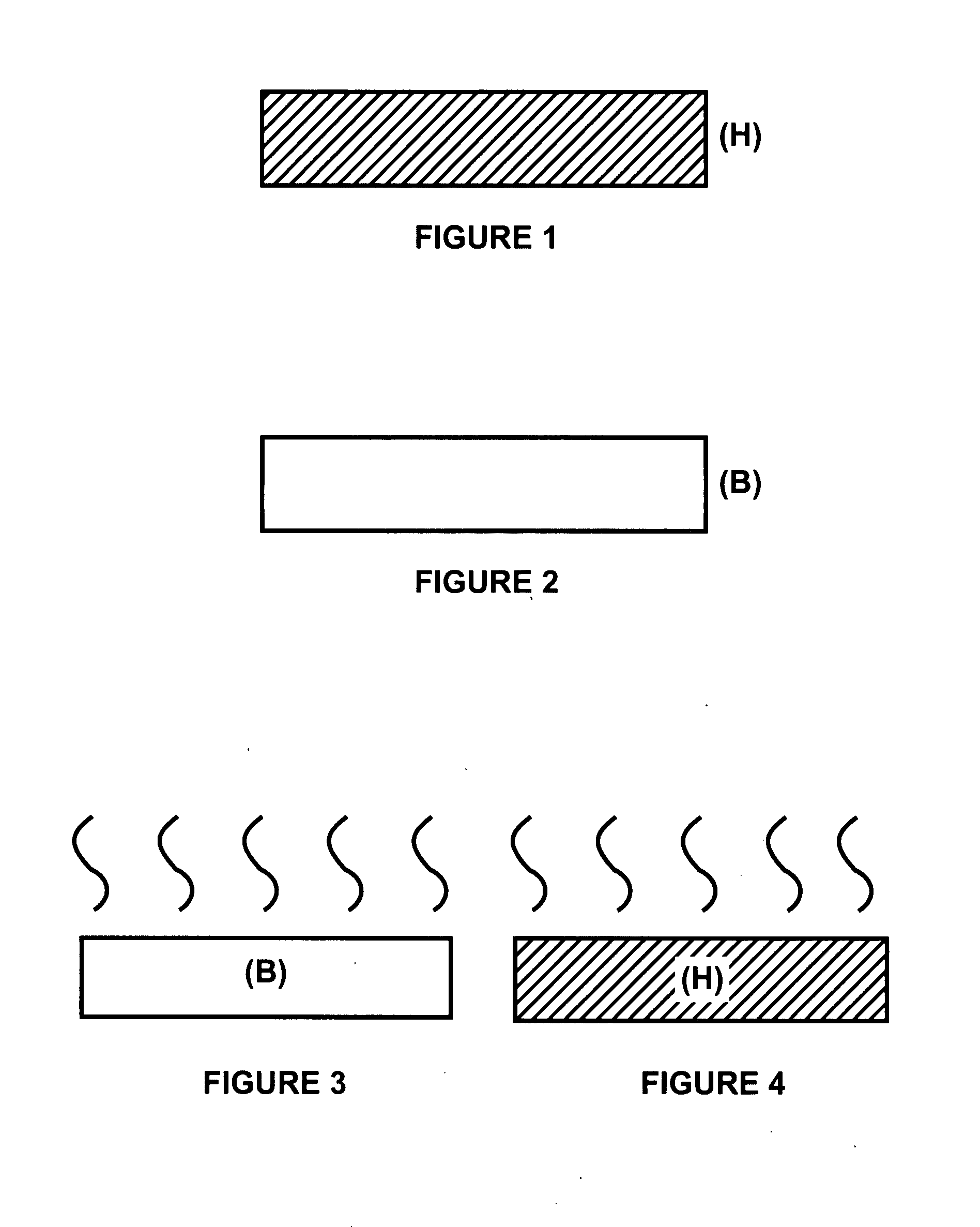
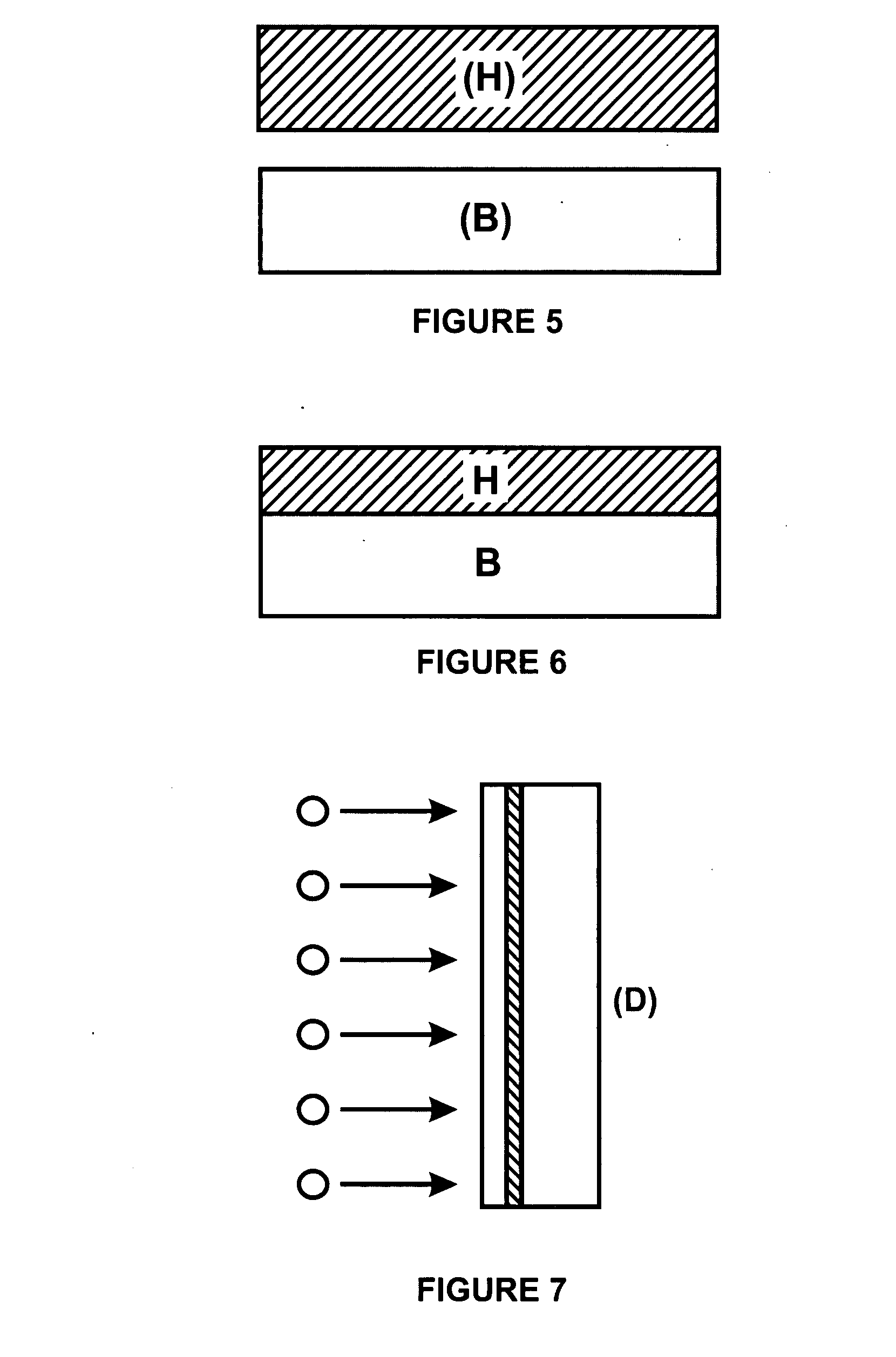
[0039]1. Provide a semiconductor substrate, which has a surface region, a cleave region and a first thickness ...


PUM

PropertyMeasurementUnit
Lengthaaaaaaaaaa
Electric potential / voltageaaaaaaaaaa

Abstract

A reusable silicon substrate device for use with layer transfer process. The device has a reusable substrate having a surface region, a cleave region, and a total thickness of material. The total thickness of material is at least N times greater than a first thickness of material to be removed. In a specific embodiment, the first thickness of material to be removed is between the surface region and the cleave region, whereupon N is an integer greater than about ten. The device also has a chuck member adapted to hold a handle substrate member in place. The chuck member is configured to hold the handle substrate in manner to facilitate bonding the handle substrate to the first thickness of material to be removed. In a preferred embodiment, the device has a mechanical pressure device operably coupled to the chuck member. The mechanical pressure device is adapted to provide a force to cause bonding of the handle substrate to the first thickness of material to be removed.

Description

CROSS-REFERENCES TO RELATED APPLICATIONS[0001]The instant nonprovisional patent application claims priority to U.S. Provisional Patent Application No. 60 / 789,730, filed Apr. 5, 2006 and incorporated by reference in its entirety herein for all purposes.BACKGROUND OF THE INVENTION[0002]Embodiments in accordance with the present invention generally relate to techniques including a method and a structure for forming a solar cell structure using layer transfer techniques for photovoltaic applications. But it will be recognized that the invention has a wider range of applicability; it can also be applied to other types of applications such as for three-dimensional packaging of integrated semiconductor devices, photonic devices, piezoelectronic devices, flat panel displays, microelectromechanical systems (“MEMS”), nano-technology structures, sensors, actuators, integrated circuits, biological and biomedical devices, and the like.[0003]From the beginning of time, human beings have relied up...

Claims


Application Information

Patent Timeline
IPC IPC(8): H01L31/18H01L21/67
CPCY10T29/41H01L31/18
Inventor HENLEY, FRANCOIS J.
Owner SILICON GENERAL CORPORATION
Why Eureka
Try Eureka