Method for fabricating an isolation layer in a semiconductor device

Inactive Publication Date: 2008-07-03
SK HYNIX INC
View PDF7 Cites 11 Cited by
  • Summary
  • Abstract
  • Description
  • Claims
  • Application Information

AI Technical Summary

Benefits of technology

[0008]In an attempt to solve the problems of the prior art, the invention provides a method for forming an isolation layer in a semiconductor device capable

Problems solved by technology

However, there is a limitation in applying such a gap-fill material and method to a trench having a low gap-fill margin due to the reduced size of the trench.
Steam annealing induces excessive oxidation in an active region and prolongs the cleaning time required to remove the remaining oxide layer.
As a result, defects (e.g., a moat) occur due to an increase in damage to the isolation layer.
In addition, loss in the substrate of the active region may ta

Method used


Image

  • Method for fabricating an isolation layer in a semiconductor device
  • Method for fabricating an isolation layer in a semiconductor device
  • Method for fabricating an isolation layer in a semiconductor device

Examples


Example

[0021]Exemplary embodiments of the invention are described in detail with reference to the accompanying drawings. In the drawings, the thickness of each element of is enlarged for clarity. Throughout the disclosure, the same or similar elements are denoted by the same reference numerals.

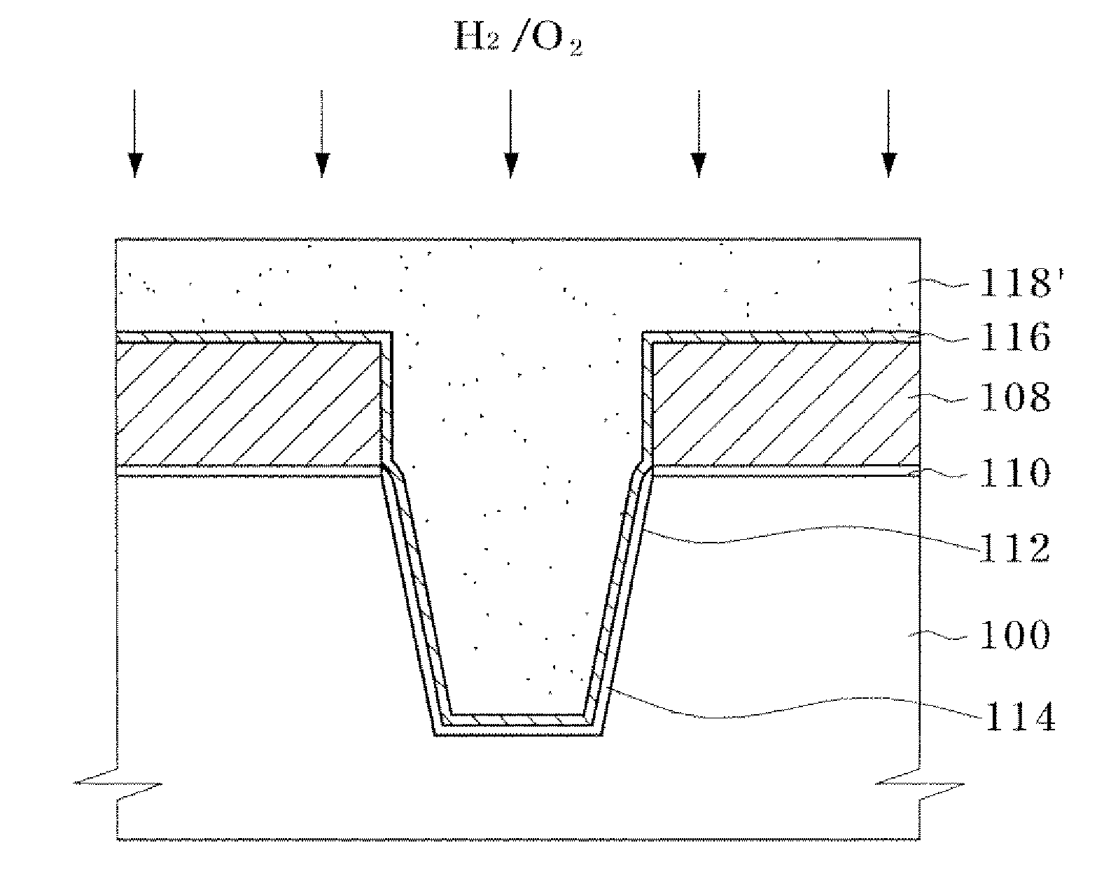
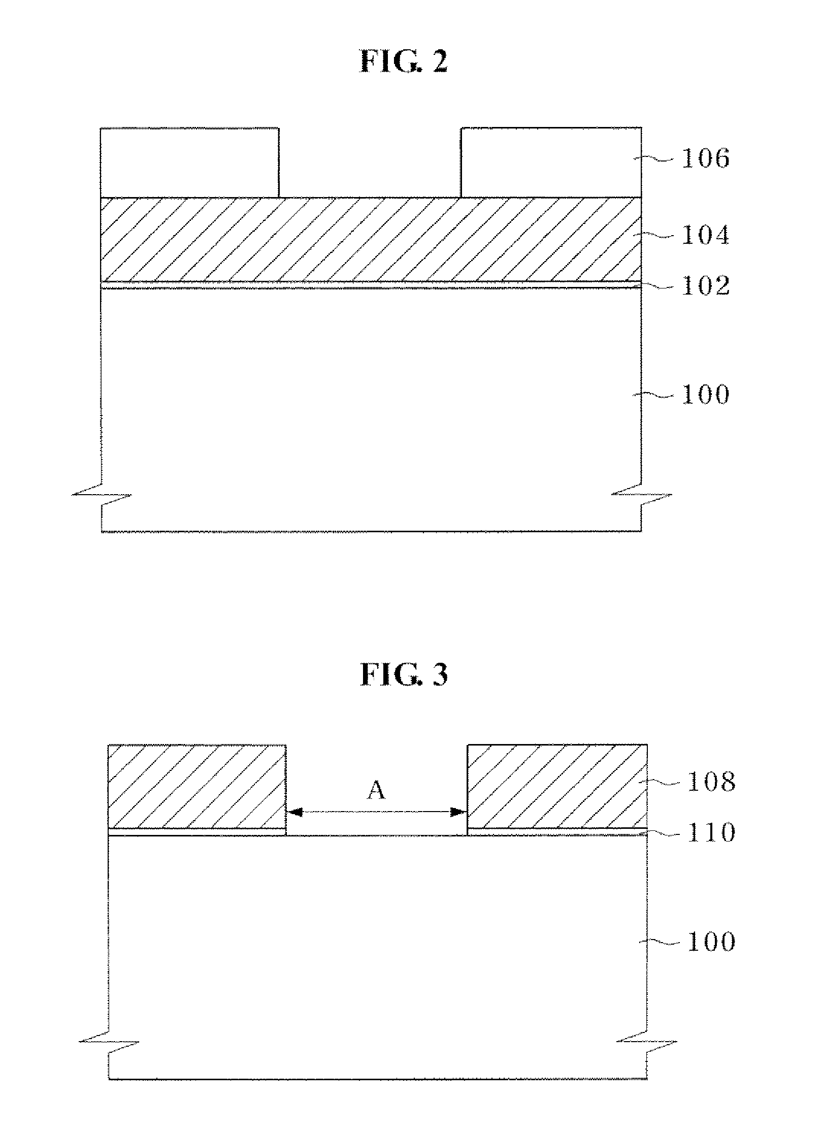
[0022]FIGS. 2 to 7 are cross-sectional views illustrating a method for forming an isolation layer in a semiconductor device according to one embodiment of the invention. FIG. 8 is a graph illustrating the variation in the etching rate as a function of time delay.

[0023]Referring to FIG. 2, a pad oxide layer 102 and a pad nitride layer 104 are sequentially deposited on a semiconductor substrate 100. Although not shown, since the pad oxide layer 102 and the pad nitride layer 104 are formed in a furnace, they are formed on the back of a wafer. The pad oxide layer 102 lessens the stress on the semiconductor substrate 100 caused by the attraction of the pad nitride layer 104. Then, a photosensitive layer (...


PUM


Abstract

A method for forming an isolation layer in a semiconductor device includes forming a trench inside a semiconductor substrate, forming a fluid insulating layer over the semiconductor substrate, thereby filling the trench with the fluid insulating layer, curing the semiconductor substrate by plasma oxidation to densify the fluid insulating layer, and planarizing the fluid insulating layer to form an isolation layer.

Description

CROSS-REFERENCE TO RELATED APPLICATION[0001]Priority to Korean patent application number 10-2006-138831, filed on Dec. 29, 2006, the disclosure of which is incorporated by reference in its entirety, is claimed.BACKGROUND OF THE INVENTION[0002]The invention relates to a semiconductor device. More specifically, the invention relates to a method for forming an isolation layer in a semiconductor device capable of ensuring stability with an improvement in the curing process for the isolation layer.[0003]In recent trends toward highly-integrated, fine-pattern semiconductor devices, there has been an increased demand for shallow trench isolation (STI) techniques exhibiting superior device isolation with a small width. The formation of an isolation layer with shallow trench isolation techniques generally includes forming a trench inside a semiconductor substrate, filling the trench with an insulating layer and planarizing the resulting structure.[0004]To improve the ability to fill the tren...

Claims


Application Information

Patent Timeline
IPC IPC(8): H01L21/762
CPCH01L21/76229H01L21/76224H01L21/762
Inventor SEO, HYE JINLEE, EUN A.LEE, AN BAE
Owner SK HYNIX INC
Why Eureka
Try Eureka