Biasing current to speed up current mirror settling time

Active Publication Date: 2008-07-10
ATMEL CORP
View PDF22 Cites 7 Cited by
  • Summary
  • Abstract
  • Description
  • Claims
  • Application Information

AI Technical Summary

Benefits of technology

[0013]According to the present invention, a method of operating a current mirror circuit including a diode-connected transistor driving a driven transistor forcing current through a load includes causing a bias current to flo

Problems solved by technology

This means that it reaches its steady-state condition in a very slow manner, in particular, in a noticeably asymptotic manner.
As a consequence, this last transient phase could take most of the total settling time.
In fact, a very low current Iin supplied to a large diode-connected transistor can result a very long asymptotic behavior of the node since the operating point is close to the turn-off point of the transistor.

Method used


Image

  • Biasing current to speed up current mirror settling time
  • Biasing current to speed up current mirror settling time
  • Biasing current to speed up current mirror settling time

Examples


Embodiment Construction

[0026]Persons of ordinary skill in the art will realize that the following description of the present invention is illustrative only and not in any way limiting. Other embodiments of the invention will readily suggest themselves to such skilled persons.

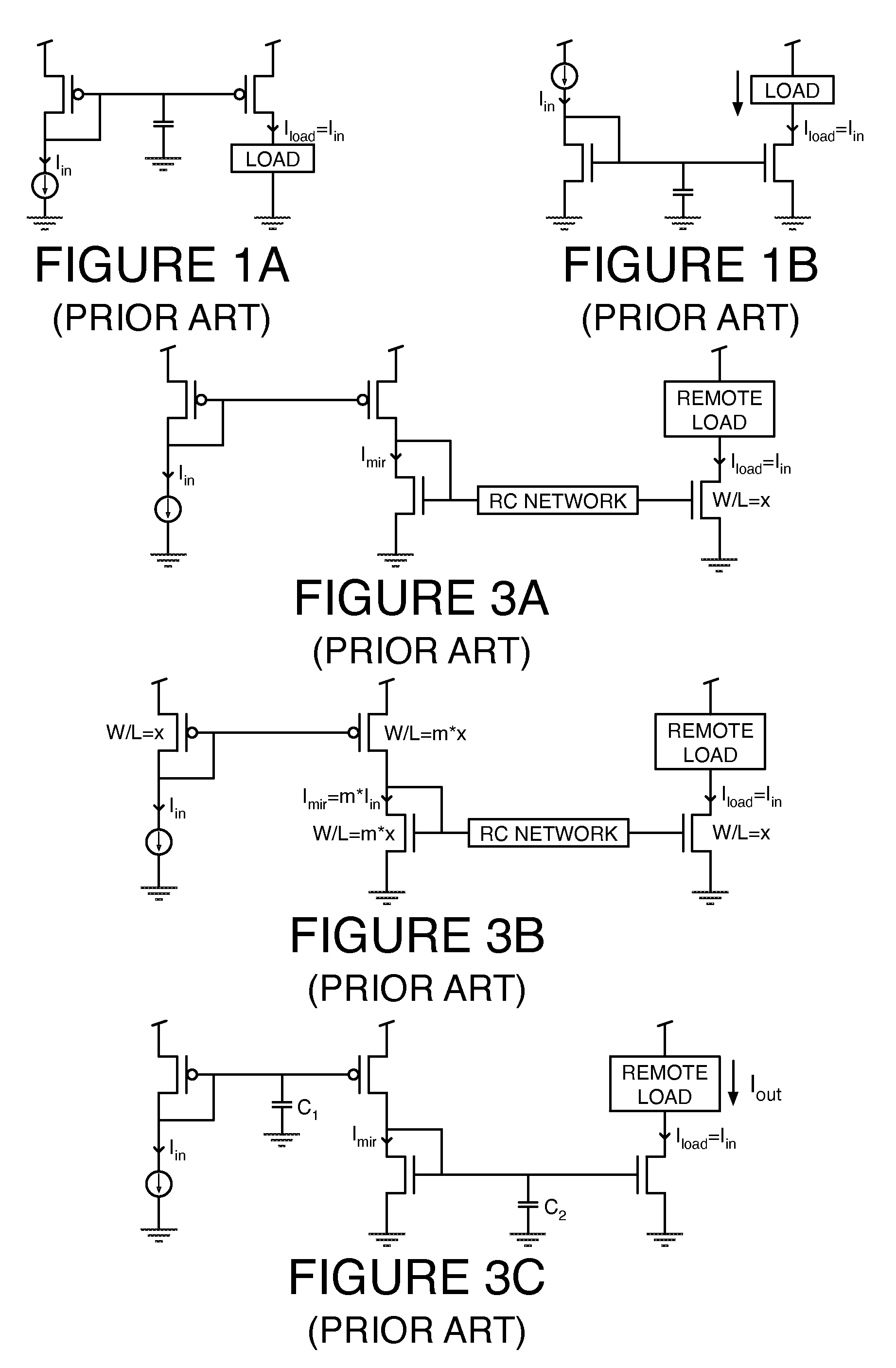
[0027]The present invention is useful for any current-mirror circuit formed from simpler p-channel and n-channel current-mirror circuits, and speeds up the settling time for a wide variety of such circuits, from the simpler to the complex.

[0028]The present invention operates by speeding up the output-current settling time, in particular, improving the last transient phase behavior of the prior-art current-mirror circuits.

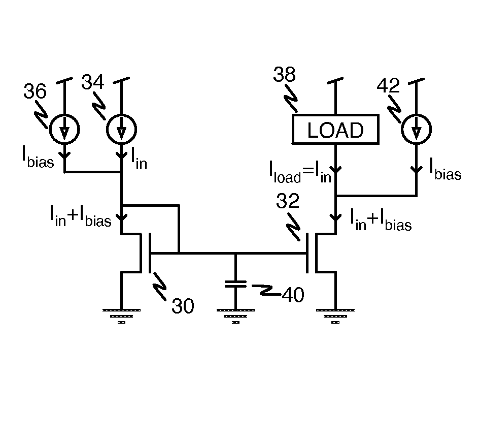
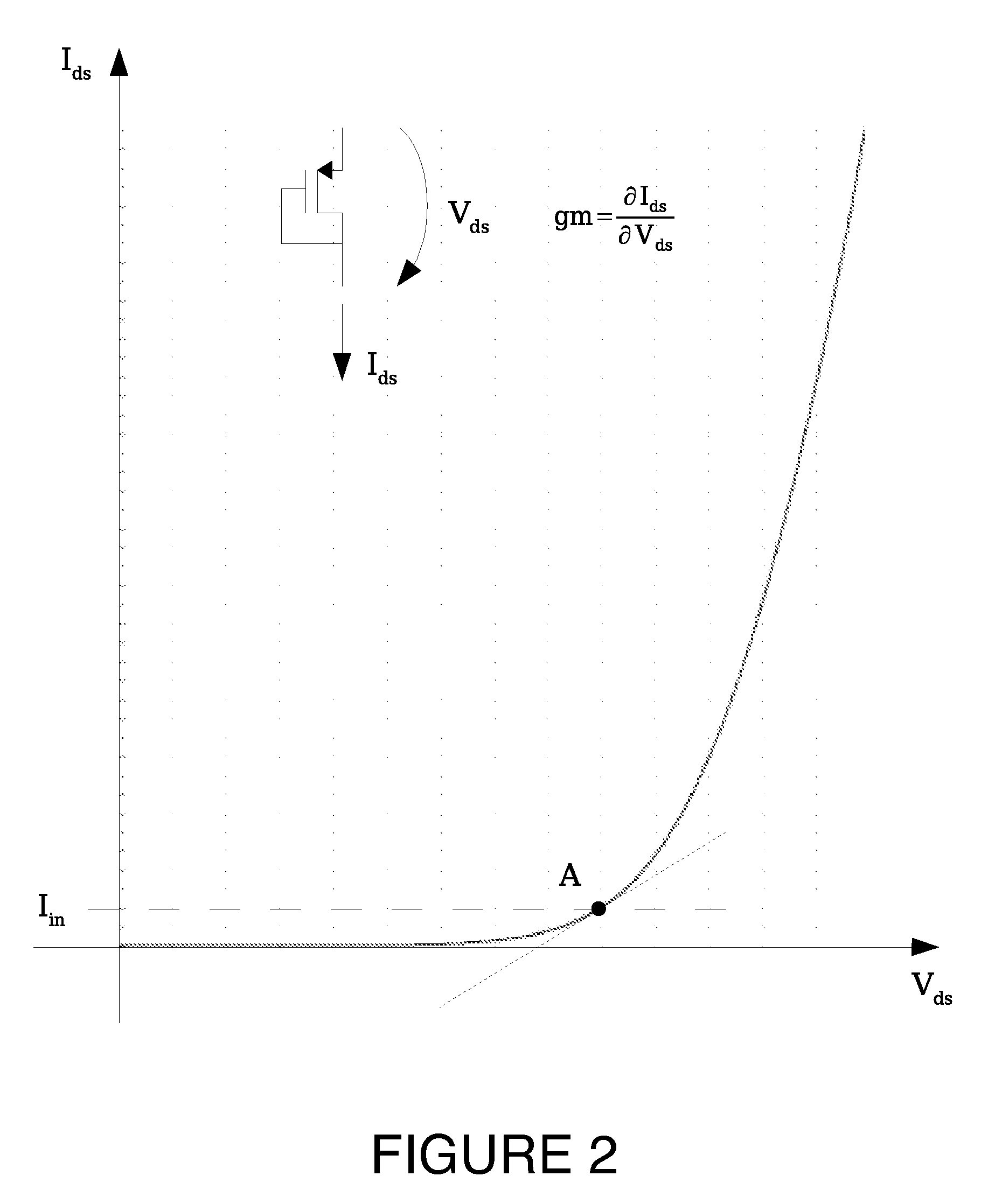
[0029]As previously noted, a significant issue of prior-art current-mirror circuits involves the operating point of the diode-connected transistor. If this transistor is designed to be larger to allow a fast initial capacitive node charging, the operating current Iin can be too low with respect to its dimensions, ther...


PUM


Abstract

A current mirror circuit includes a first current-mirror transistor coupled to a second current-mirror transistor. A load is coupled to the second current-mirror transistor. A first current source is coupled to the first current-mirror transistor to cause a bias current to flow through the first current-mirror transistor and a second current source is coupled to the second current-mirror transistor and in parallel with the load to shunt the bias current away from the load.

Description

BACKGROUND OF THE INVENTION[0001]1. Field of the Invention[0002]The present invention relates to current mirror circuits. More particularly, the present invention relates to a current-mirror circuit including a biasing current to speed up current-mirror settling time[0003]2. The Prior Art[0004]Simple prior-art current-mirror circuits are shown in FIGS. 1A and 1B. The circuit of FIG. 1A transfers the input current Iin to a load circuit by two p-channel mirror-connected transistors. The current generator schematically represents any generic current source that supplies the input current to the mirror connected transistors, and the capacitance represents any possible load capacitance associated with the node connecting together the gates of the two transistors. In FIG. 1B, an equivalent circuit using two n-channel mirror-connected transistors is shown. The two circuits are equivalent from an operation point of view. By changing the ratio of the dimensions of the mirror-connected transi...

Claims


Application Information

Patent Timeline
IPC IPC(8): H03F3/04
CPCH03F3/343G09G3/3225G09G3/3216G09G3/20
Inventor PELLI, GABRIELEBEDARIDA, LORENZOFRULIO, MASSIMILIANOBETTINI, ANDREA
Owner ATMEL CORP
Why Eureka
Try Eureka