System and method for providing slew rate enhancement for two stage CMOS amplifiers

a technology of complementary metal oxide semiconductors and amplifiers, which is applied in the direction of amplifiers with semiconductor devices/discharge tubes, amplifier details, differential amplifiers, etc., can solve the problems of difficult to prevent the extra circuitry from degrading the electrical characteristics of the underlying operational amplifier, the bias boost method is not desirable for two stage cmos amplifiers, and the need for extra circuitry

Active Publication Date: 2008-04-22
NAT SEMICON CORP
View PDF1 Cites 30 Cited by
  • Summary
  • Abstract
  • Description
  • Claims
  • Application Information

AI Technical Summary

Problems solved by technology

The Bias Boost approach necessarily requires extra circuitry.
It is sometimes very difficult to prevent the extra circuitry from degrading the electrical characteristics of the underlying operational amplifier.
The Bias Boost method is not desirable for two stage CMOS amplifiers.
The Bias Boost method is not compatible with some commonly used operational amplifier architectures.
The Load Boost method is not desirable for two stage CMOS amplifiers.
The Load Boost method is deficient because pos

Method used


Image

  • System and method for providing slew rate enhancement for two stage CMOS amplifiers
  • System and method for providing slew rate enhancement for two stage CMOS amplifiers
  • System and method for providing slew rate enhancement for two stage CMOS amplifiers

Examples


Embodiment Construction

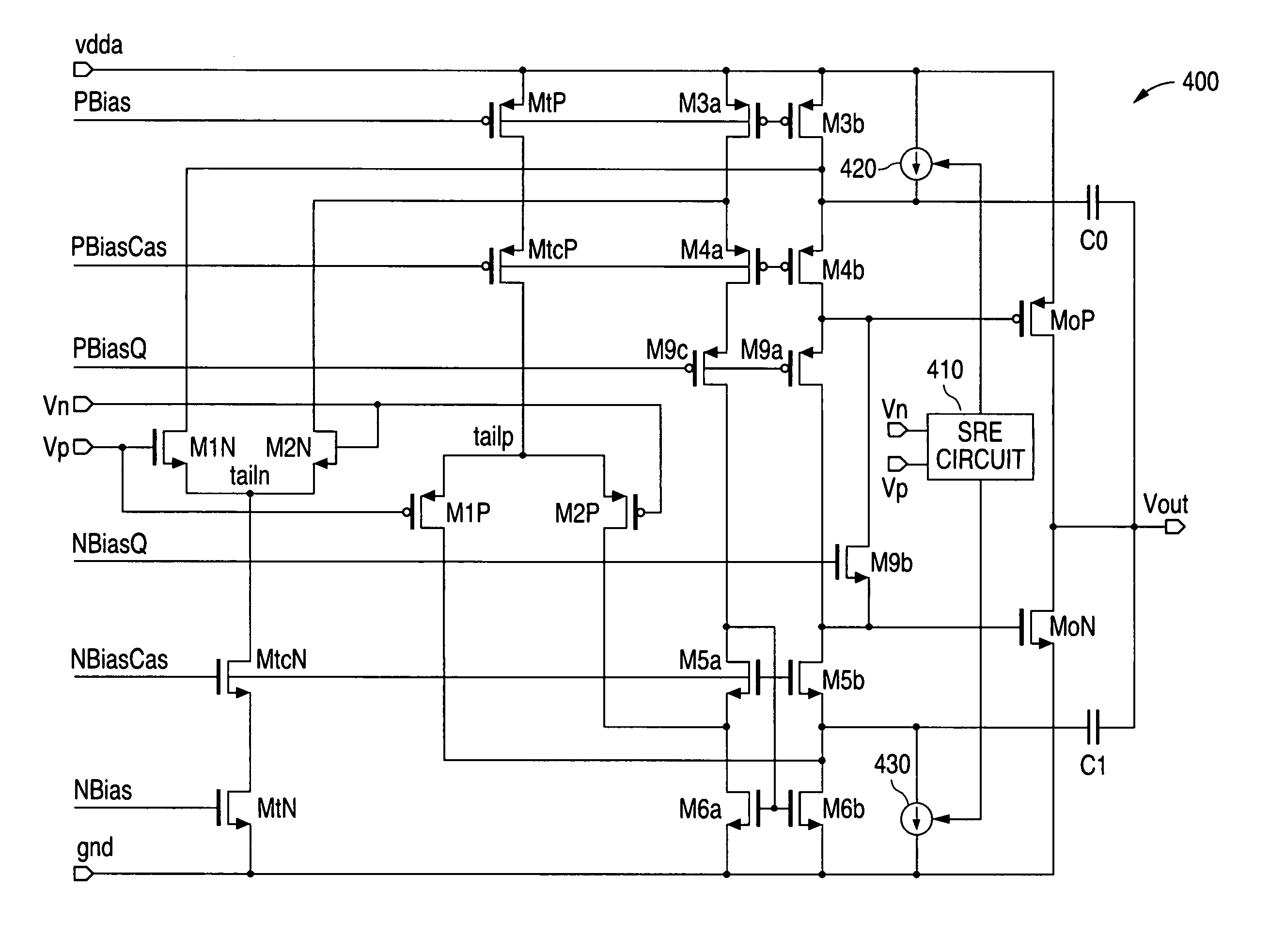
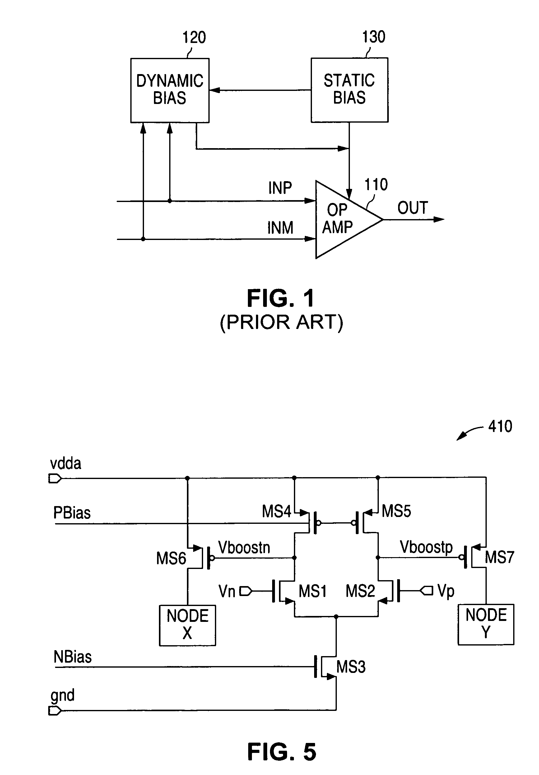
[0026]FIGS. 3 through 10, discussed below, and the various embodiments used to describe the principles of the present invention in this patent document are by way of illustration only and should not be construed in any way to limit the scope of the invention. Those skilled in the art will understand that the principles of the present invention may be implemented in any type of suitably arranged two stage CMOS operational amplifier circuit.

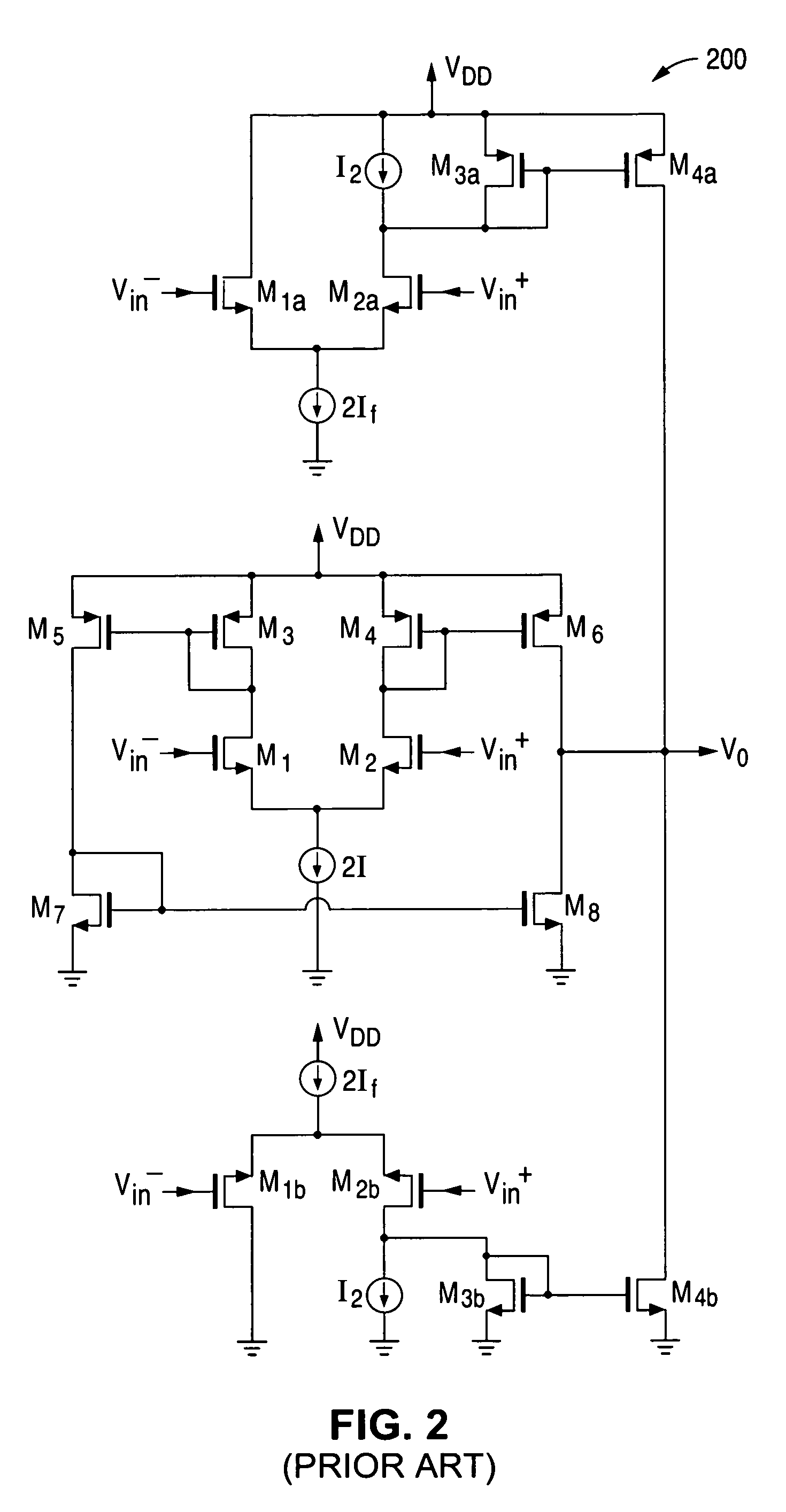
[0027]FIG. 3 illustrates a prior art operational amplifier circuit 300. Operational amplifier circuit 300 comprises a first stage and a second stage. The first stage of operational amplifier circuit 300 comprises a folded cascode circuit with a dual polarity front end. The second stage of operational amplifier circuit 300 comprises a class AB common source stage. The compensation method employed in operational amplifier circuit 300 is a cascoded Miller compensation.

[0028]FIG. 4 illustrates an operational amplifier circuit 400 constructed in accorda...


PUM


Abstract

A slew rate enhancement circuit is disclosed for increasing a slew rate in a two stage CMOS amplifier. The slew rate enhancement circuit detects an input signal transition in the two stage CMOS amplifier. Depending on the polarity of the input signal transition the slew rate enhancement circuit turns on either (1) a first current source to charge a first compensation capacitor, or (2) a second current source to charge a second compensation capacitor. The slew rate enhancement circuit increases the slew rate by a factor of four to five and decreases the settling time of a voltage transition by a factor of three.

Description

CROSS-REFERENCE TO RELATED APPLICATION[0001]This application claims the benefit of priority under 35 U.S.C. §119(e) (1) of provisional application Ser. No. 60 / 717,989 filed on Sep. 16, 2005, which is incorporated herein by reference for all purposes.TECHNICAL FIELD OF THE INVENTION[0002]The present invention is generally directed to manufacturing technology for semiconductor devices and, in particular, to circuitry for providing slew rate enhancement for two stage complementary metal oxide semiconductor (CMOS) amplifiers.BACKGROUND OF THE INVENTION[0003]In an operational amplifier circuit the slew rate is a measure of the variation in the output voltage in terms of volts per unit time. The higher the slew rate, the quicker an output voltage of the operational amplifier can reach a desired target voltage value. It is therefore desirable to maximize the slew rate in an operational amplifier circuit.[0004]Two different types of approaches have been taken to increase the slew rate in si...

Claims


Application Information

Patent Timeline
IPC IPC(8): H03F3/45H03F1/14
CPCH03F3/4521H03F2203/45091H03F2203/45248H03F2203/45512
Inventor KNAUSZ, IMRE
Owner NAT SEMICON CORP
Why Eureka
Try Eureka