Reference generator circuit and method for nonvolatile memory devices

a reference generator and memory device technology, applied in the direction of digital storage, process and machine control, instruments, etc., can solve the problems of large integration effect, large surface area of silicon, and relative small silicon area,

Inactive Publication Date: 2004-03-16
STMICROELECTRONICS SRL
View PDF15 Cites 31 Cited by
  • Summary
  • Abstract
  • Description
  • Claims
  • Application Information

AI Technical Summary

Problems solved by technology

This results in a relatively small silicon area and the effectuation of large scale integration.
The tradeoff here is that a larger surface area of silicon is required and therefore a smaller scale of integration is achieved.
There is a relatively slow settling time of the reference voltage due to the large capacitive loading on the reference current generator / mirror circuit when a large number of sense amplifiers are used.
In addition, the limitation exists due to the amount of noise introduced within each sense amplifier that may affect data integrity.
As a result, certain flash memory device features, such as burst mode and page mode features, cannot be effectively executed in conventional flash memory devices.

Method used


Image

  • Reference generator circuit and method for nonvolatile memory devices
  • Reference generator circuit and method for nonvolatile memory devices
  • Reference generator circuit and method for nonvolatile memory devices

Examples


Embodiment Construction

The present invention will now be described more fully hereinafter with reference to the accompanying drawings in which an exemplary embodiment of the invention is shown. This invention may, however, be embodied in many different forms and should not be construed as being limited to the embodiment set forth herein. Rather, the embodiment is provided so that this disclosure will be thorough and complete, and will fully convey the scope of the invention to those skilled in the art.

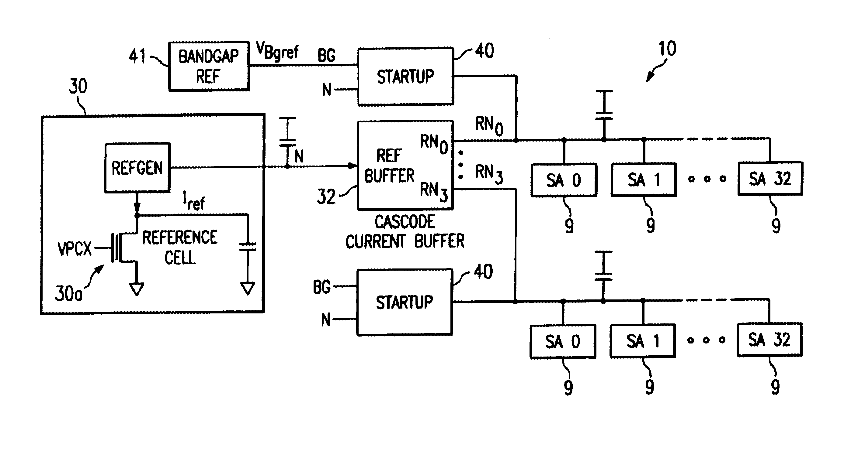
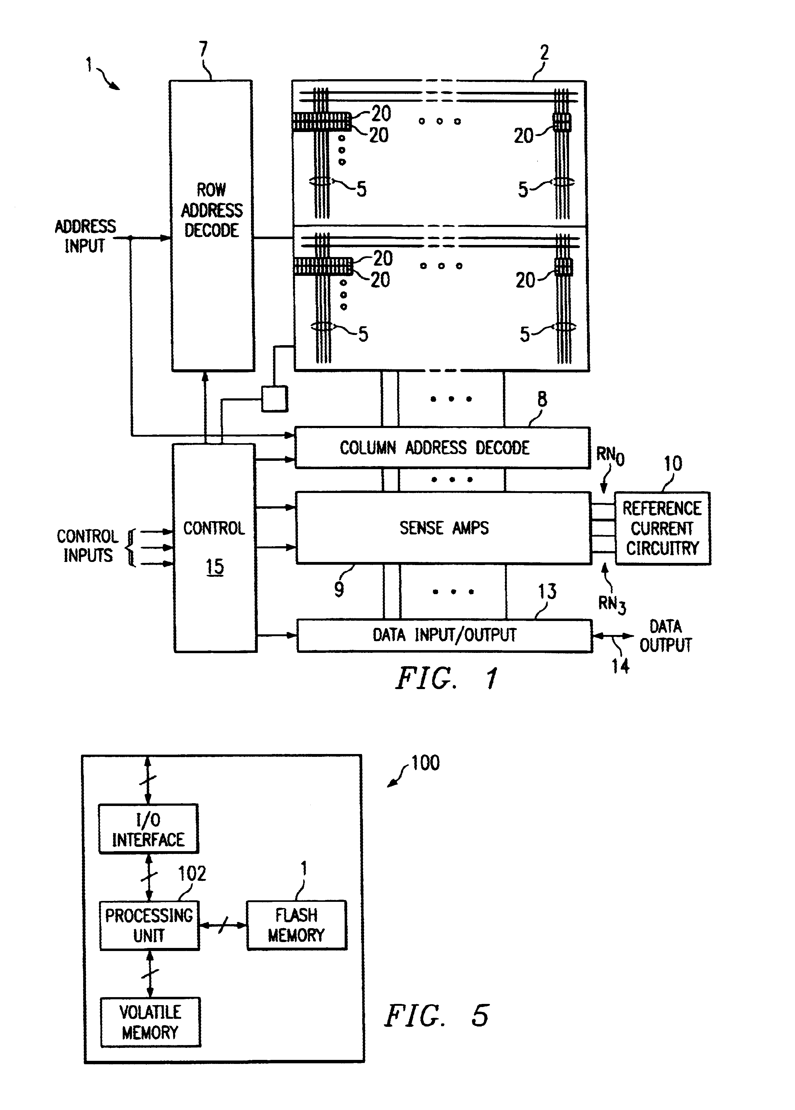
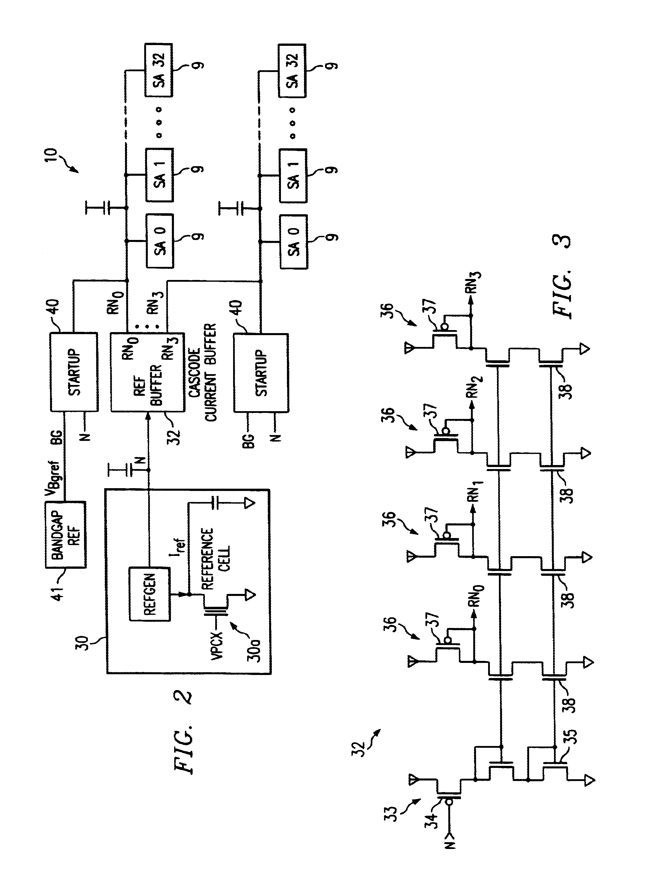
Referring to FIGS. 1-4, there is disclosed a nonvolatile memory device 1 according to an exemplary embodiment of the present invention. It is understood that memory device 1 may be any type of nonvolatile memory device, such as a flash memory device. Memory device 1 will be described below as a flash memory device for reasons of simplicity.

Flash memory device 1 includes one or more arrays or banks 2 of memory cells 20. Each array 2 of memory cells 20 may be arranged into rows and columns of memory cells 20. ...


PUM


Abstract

Reference generator circuitry for providing a reference to sense amplifiers in a flash memory device. The circuitry includes a reference current generator for generating a reference current for use by the sense amplifier circuits. A current buffer circuit in the flash memory device mirrors the reference current and applies a plurality of mirrored reference currents to the reference inputs of the sense amplifiers. A startup circuit is utilized in order to provide a fast settling time of the reference node appearing at the input of the sense amplifiers. The startup circuit includes first and second discharge current stages, with the first discharge current stage discharging the charge appearing at the reference node input of the sense amplifiers based upon a bandgap reference current. The second discharge current stage discharging the charge appearing at the reference node input of the sense amplifiers based upon the reference current. Each discharge current stage utilizes feedback to gradually decrease the rate of discharge by the discharge current stage so that the discharge current stages are disabled by the time the voltage appearing at the reference node input of the sense amplifiers reaches the desired voltage level.

Description

1. Technical Field of the InventionThe present invention relates to a reference current generator for memory devices, and particularly to circuitry for more effectively generating a reference current in nonvolatile memory devices.2. Description of the Related ArtThe first nonvolatile memories were electrically programmable read-only memories (EPROMs). In these memories, the memory cells include a floating-gate transistor that is programmable using the hot carrier effect. Programming of an EPROM memory cell includes applying a potential difference between the drain and the source of the floating gate transistor in the presence of a high potential difference (of about 20 volts, this value varying according to the desired programming speed) between the control gate and the source. The application of the first of these potential differences generates an electrical field that gives rise to a flow of electrons in the channel. These electrons collide with atoms of the channel, causing the ...

Claims


Application Information

Patent Timeline
Patent Type & Authority Patents(United States)
IPC IPC(8): G11C5/14G11C7/00G11C7/14G11C16/06G11C16/28G05F3/26
CPCG11C5/147G11C7/14G11C16/28
Inventor MICHAEL, ORONSEVER, ILAN
Owner STMICROELECTRONICS SRL
Why Eureka
Try Eureka