Three-dimensional architecture for self-checking and self-repairing integrated circuits

a three-dimensional architecture and integrated circuit technology, applied in the direction of electrical apparatus, electrical apparatus contruction details, semiconductor devices, etc., can solve the problems of wasting several clock cycles, and affecting the recovery and state rollback of the last correct sta

Inactive Publication Date: 2008-07-10
IBM CORP
View PDF6 Cites 161 Cited by
  • Summary
  • Abstract
  • Description
  • Claims
  • Application Information

AI Technical Summary

Problems solved by technology

Otherwise, several clock cycles are wasted during which erroneous instruction and data information are spread throughout the system.
This would make recovery and state rollback to a last correct state very difficult given the exponential growth of a fault tree.
The problem with bringing fault-detection, repair, and recovery functions to the hardware level is the negative impact that implementing such circuitry has on chip area, wireability, and performance of the overall chip.

Method used


Image

  • Three-dimensional architecture for self-checking and self-repairing integrated circuits
  • Three-dimensional architecture for self-checking and self-repairing integrated circuits
  • Three-dimensional architecture for self-checking and self-repairing integrated circuits

Examples


Embodiment Construction

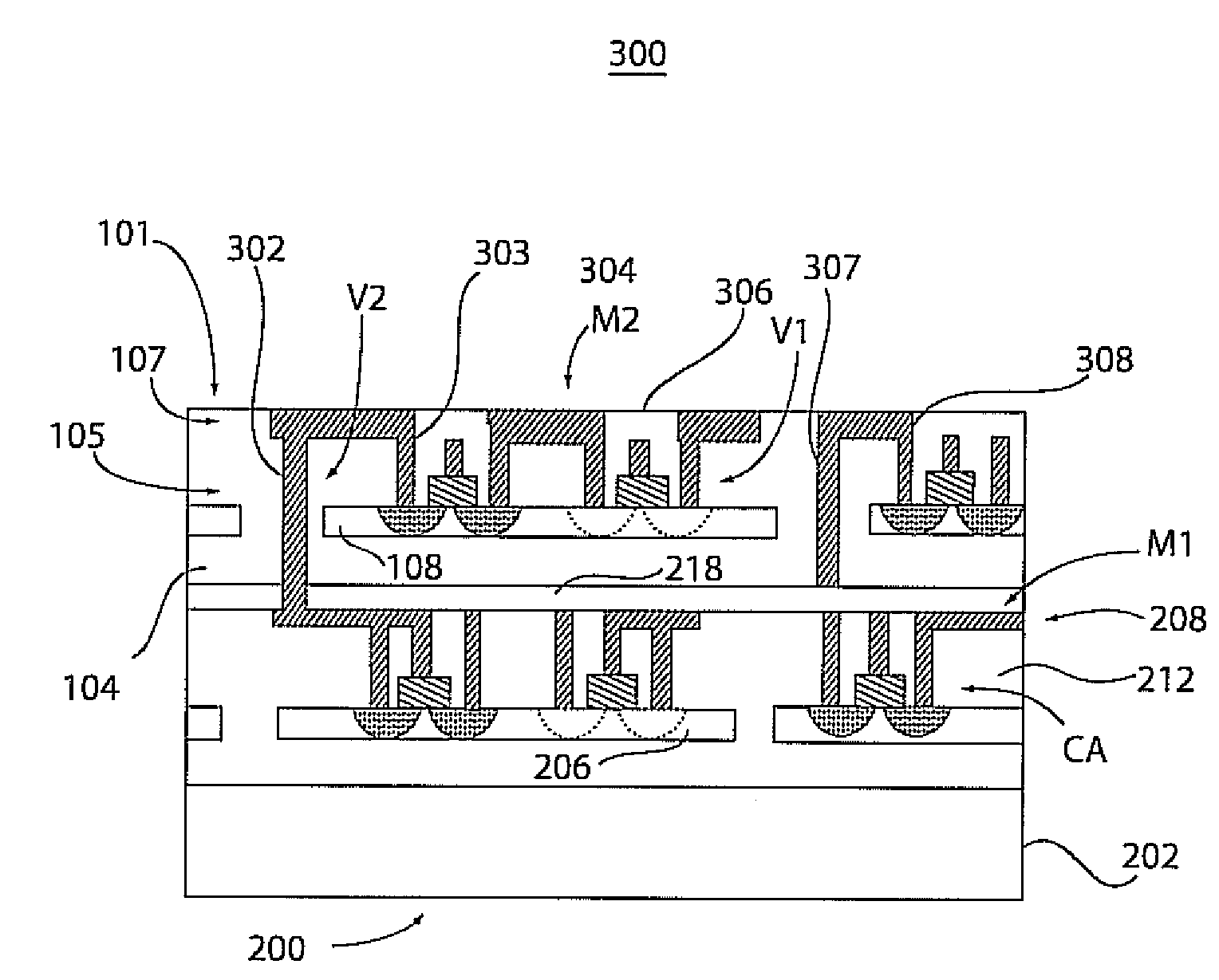
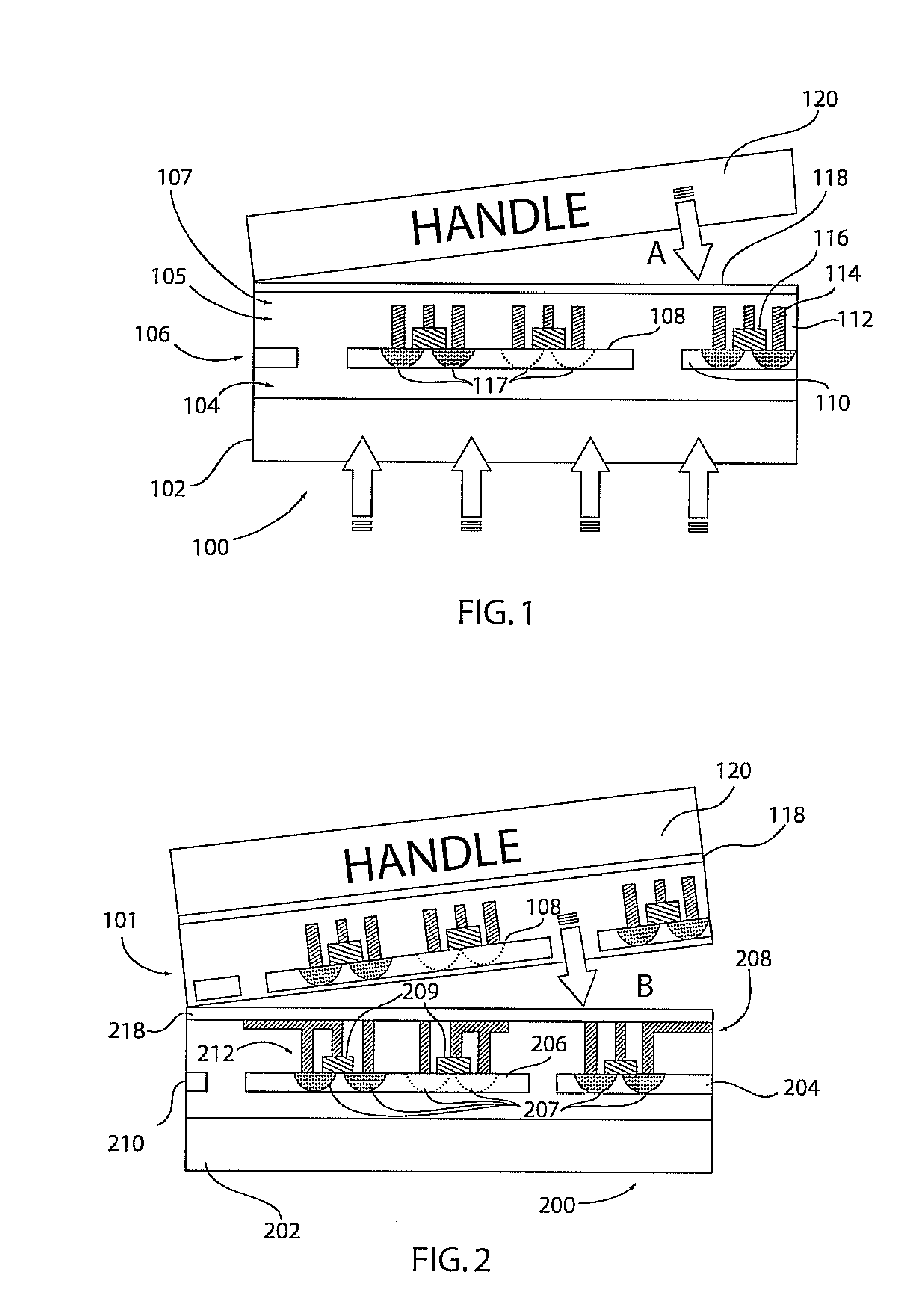
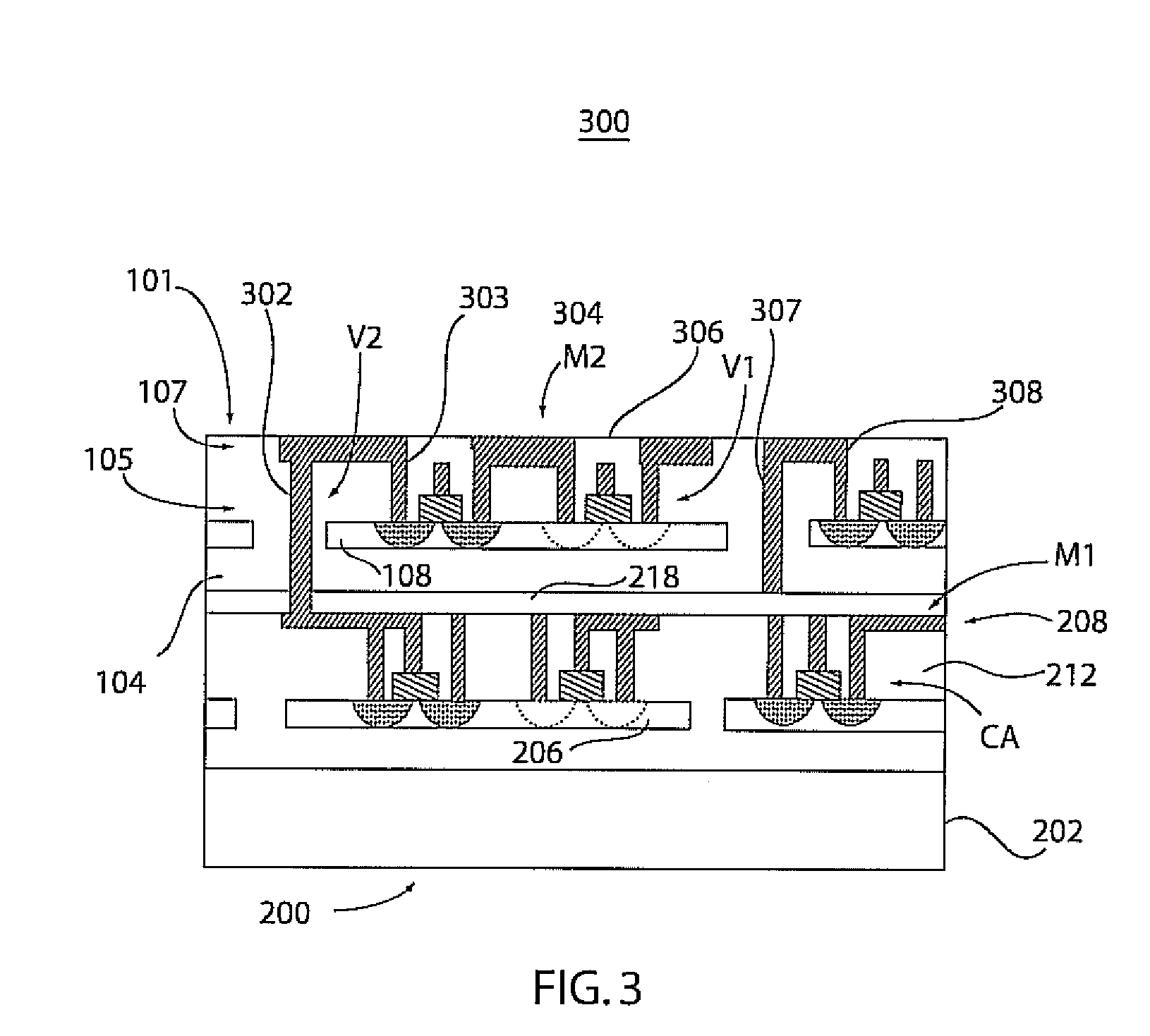
[0019]Embodiments in accordance with present principles preferably employ the manufacturing of three-dimensional chips by bonding several active layers in one stack along with interconnect level connection between each portion of the stack. For present purposes, a chip may be defined as an integrated circuit including one more passive or active elements. A stack includes two or more chips operatively coupled to each other to perform an operation. A stack may be referred to as having a three-dimensional architecture or as a three-dimensional chip, since the stack employs not only a layout area but a stack height. Separately fabricated refers two chips fabricated separately in different processes and perhaps remote locations.

[0020]In accordance with present principles, fabrication and manufacturing methods are employed to take advantage of the stacking capabilities in designing fault-detection, repair, and recovery circuits that run concurrently with monitored hardware. Design and arc...


PUM


Abstract

A three-dimensional architecture chip includes a base chip including a unit integrated thereon and configured to perform electrical signal operations. An active layer is separately fabricated from the base layer. The active layer includes a component to service the unit of the base chip. The active layer is bonded to the base chip such that the component is aligned in vertical proximity of the unit. An electrical connection connects the unit to the component through vertical layers of at least one of the base chip and the active layer.

Description

GOVERNMENT RIGHTS[0001]This invention was made with Government support under Contract No.: N66001-04-C-8032 awarded by the Defense Advanced Research Projects Agency (DARPA). The Government has certain rights in this invention.BACKGROUND[0002]1. Technical Field[0003]The present invention relates to circuit architectures and more particularly to circuit designs employing semiconductor stacks having power circuits, self-repairing circuits, self-checking circuits or other integrated circuits advantageously positioned in the stack.[0004]2. Description of the Related Art[0005]Reliability, availability and serviceability (RAS) of complex integrated circuits, such as high performance microprocessors, require that fault detection and repair actions happen immediately after fault occurrence. Otherwise, several clock cycles are wasted during which erroneous instruction and data information are spread throughout the system. This would make recovery and state rollback to a last correct state ver...

Claims


Application Information

Patent Timeline
Patent Type & Authority Applications(United States)
IPC IPC(8): H05K7/00H01L21/50
CPCH01L21/6835H01L2924/01006H01L24/26H01L24/83H01L25/0657H01L25/18H01L25/50H01L27/0688H01L2221/68354H01L2224/8385H01L2225/06524H01L2225/06541H01L2924/01005H01L2924/07802H01L2924/14H01L2924/19041H01L2924/19042H01L2924/19043H01L21/8221
Inventor BERNSTEIN, KERRYCOTEUS, PAUL WILLIAMELFADEL, IBRAHIM (ABE) M.EMMA, PHILIP GEORGEGUARINI, KATHRYN W.FLEISCHMAN, THOMASHARTSTEIN, ALLAN MARKPURI, RUCHIRRITTER, MARK B.TREWHELLA, JEANNINE MADELYNYOUNG, ALBERT M.
Owner IBM CORP
Why Eureka
Try Eureka