Light-emitting diode

a diode and light-emitting technology, applied in the direction of basic electric elements, semiconductor devices, electrical equipment, etc., can solve the problems of low brightness, low extraction efficiency of conventional leds, and loss of most of light rays emitted within leds, and achieve high extraction efficiency

Inactive Publication Date: 2008-07-17
TSINGHUA UNIV +1
View PDF4 Cites 83 Cited by
  • Summary
  • Abstract
  • Description
  • Claims
  • Application Information

AI Technical Summary

Benefits of technology

[0010]Compared with a conventional LED, the present LED has high extraction efficiency, e.g., up to about 50% with a simple configure, that is, a second diffraction grating. The periods of the diffraction grating are comparable with the wavelength of light rays emitted from the LED, and thus the LED can be manufracted by a conventional etch technology. Therefore, the present LED is easy to manufract at low lost.

Problems solved by technology

However, most of the light rays emitted within an LED are lost due to total internal reflection at the LED-air interface.
Therefore, the conventional LED has low extraction efficiency, and then has low brightness.

Method used


Image

  • Light-emitting diode
  • Light-emitting diode
  • Light-emitting diode

Examples


first embodiment

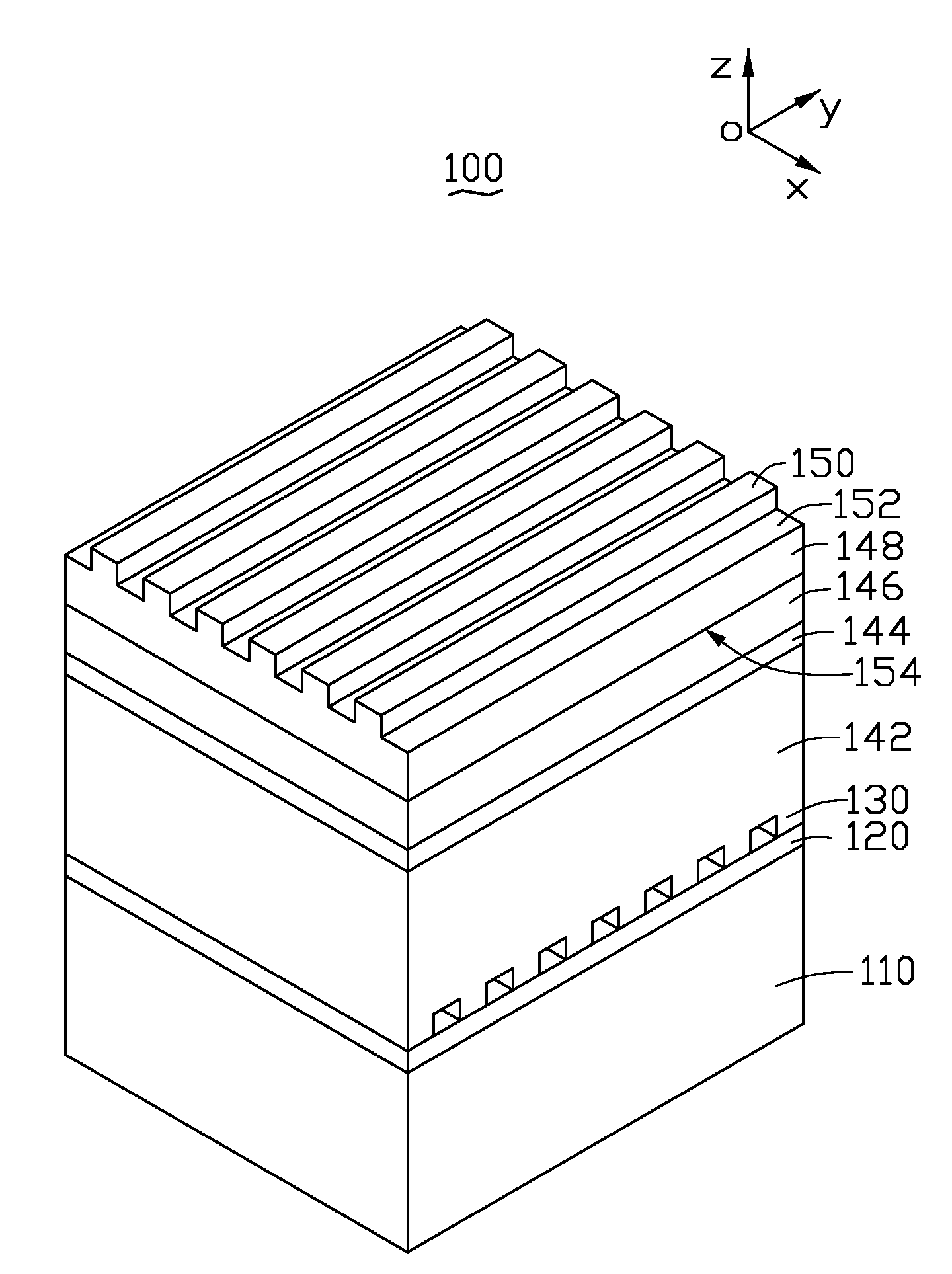
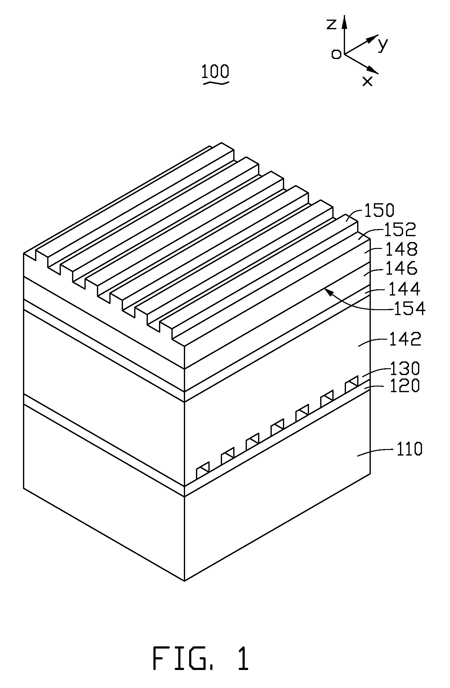
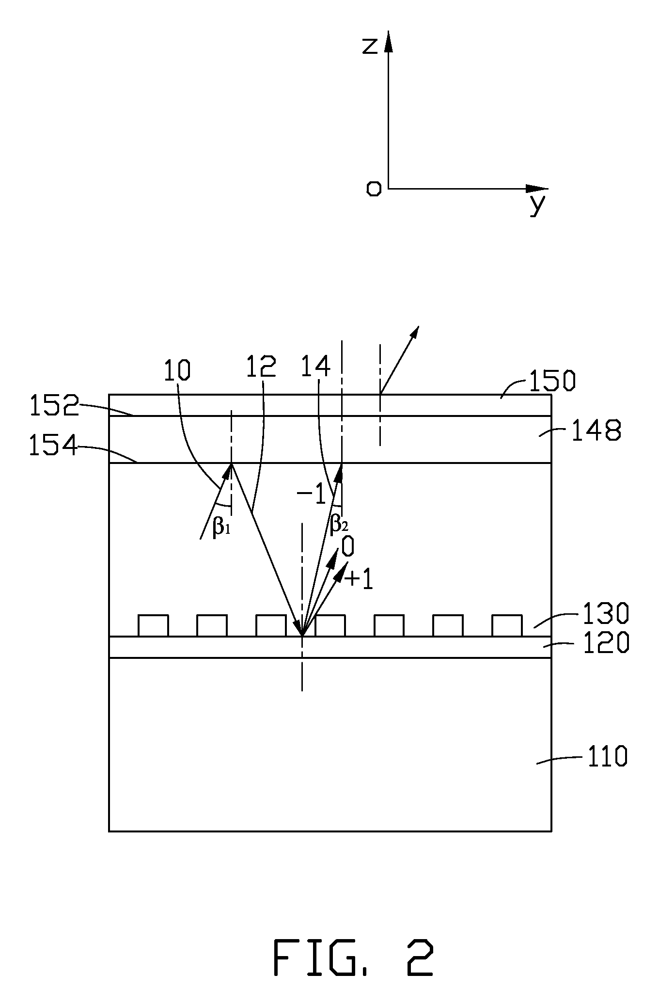
[0017]Referring to FIG. 1, an LED 100, is shown. The LED 100 includes a substrate 110, a reflective layer 120, an N-type semiconductor layer 142, an active layer 144, a P-type semiconductor layer 146, a transparent electrode layer 148, a first diffraction grating 150 and a second diffraction grating 130. The substrate 110, the reflective layer 120, the second diffraction grating 130, the N-type semiconductor layer 142, the active layer, the P-type semiconductor layer 146, the transparent electrode and the first diffraction grating are arranged in the order, i.e., typically disposed in stack.

[0018]The reflective layer 120 is deposited on the substrate 110, or selectively, on the surface of the second diffraction grating 130. The reflective layer 120 functions as a mirror and an electrode. The transparent electrode layer 148 includes a top surface 152 and a bottom surface 154. The bottom surface 154 is connected with the P-type semiconductor layer 146, and the top surface 152 is conn...

second embodiment

[0025]Referring to FIG. 3, an LED 200 is shown. The LED 200 includes a substrate 210, a reflective layer 220, a second diffraction grating 230, an N-type semiconductor layer 242, an active layer 244, a P-type semiconductor layer 246, a transparent electrode layer 248 and a first diffraction grating 250 typically disposed in stack. The LED 200 is similar to the LED 100, except that the grooves of the first diffraction grating 250 are parallel to that of the second diffraction grating 230. The light extraction efficiency of the LED 200 is about 28.6%, higher than that of the conventional LED with only the first diffraction grating.

[0026]It is known to the one killed in the field than the LED also can include a substrate, a reflective layer, a second diffraction grating, a P-type semiconductor layer, an active layer, an N-type semiconductor layer, a transparent electrode layer and a first diffraction grating disposed in stack. Further, the substrate can be removed, and the reflective ...


PUM


Abstract

A light-emitting diode includes a substrate (110), a reflective layer (120), a second diffraction grating (130), a first semiconductor layer (142), an active layer (144), a second semiconductor layer (146), a transparent electrode layer (148), and a first diffraction grating (150), arranged in that order. The first diffraction grating and the second diffraction grating is composed of an array of parallel and equidistant grooves, and a inclined angle between the grooves of the first diffraction grating and the grooves of the second diffraction grating is equal to or more than 0° and equal to or less than 90°. One of the first semiconductor layer and the second semiconductor layer is an N-type semiconductor and the other thereof is a P-type semiconductor. The light-emitting diode has high light extraction efficiency and is easy to manufacture at a low cost.

Description

BACKGROUND[0001]1. Field of the Invention[0002]The present invention relates to light-emitting devices and, particularly, to a light-emitting diode (LED).[0003]2. Discussion of Related Art[0004]LEDs are semiconductors that convert electrical energy into light. Compared to conventional light sources, the LEDs have higher energy conversion efficiency, higher radiance (i.e., they emit a larger quantity of light per unit area), longer lifetime, higher response speed, and better reliability. At the same time, LEDs generate less heat. Therefore, LED modules are widely used in particular as a semiconductor light source in conjunction with imaging optical systems, such as displays, projectors, and so on.[0005]A conventional LED includes a substrate, a first electrode layer formed on the substrate, an N-type semiconductor layer, an active layer, a P-type semiconductor layer and a second electrode layer typically disposed in stack. In operation, a voltage is applied between the first electrod...

Claims


Application Information

Patent Timeline
Patent Type & Authority Applications(United States)
IPC IPC(8): H01L33/00H01L33/10H01L33/20H01L33/38
CPCH01L33/10H01L2933/0083H01L33/38H01L33/20
Inventor XU, ZHEN-FENGJIN, GUO-FANFAN, SHOU-SHAN
Owner TSINGHUA UNIV
Why Eureka
Try Eureka