Stacked structure of semiconductor devices, semiconductor device package, and methods of fabricating the same

Active Publication Date: 2008-07-17
SAMSUNG ELECTRONICS CO LTD
View PDF6 Cites 32 Cited by
  • Summary
  • Abstract
  • Description
  • Claims
  • Application Information

AI Technical Summary

Benefits of technology

[0017]A stacked structure of semiconductor devices may include a plurality of stacked semiconductor devices, each having an upper surface with bonding pads and a lower surface opposite to the upper surface. One or more via-electrodes may be connected to the bonding pads and may have upper parts (heads) protruding from the upper surface and lower parts (ends) protruding from the lower surface. A first adhesive film may be on the upper surface of the semiconductor devices and may be substantially level with the protruding heads of the via-electrodes. The first adhesive film may include a patternable material having first patterning properties and first puncturing properties. The first adhesive film may include at least one of a novolak, benzocyclobutene (BCB), polyimide, and epoxy.

Problems solved by technology

However, such two-dimensional integration of the memory cells may require the use of more advanced technology, including microscopic line widths, and/or longer development terms.
As a result, adhesion between the adhesive film 30a and the lower surface of the semiconductor device 20b may not be sufficient, thereby decreasing the reliability of the stacked structure.
The adhesive film 60a may have improved adhesive properties because of its increased bonding

Method used


Image

  • Stacked structure of semiconductor devices, semiconductor device package, and methods of fabricating the same
  • Stacked structure of semiconductor devices, semiconductor device package, and methods of fabricating the same
  • Stacked structure of semiconductor devices, semiconductor device package, and methods of fabricating the same

Examples


Embodiment Construction

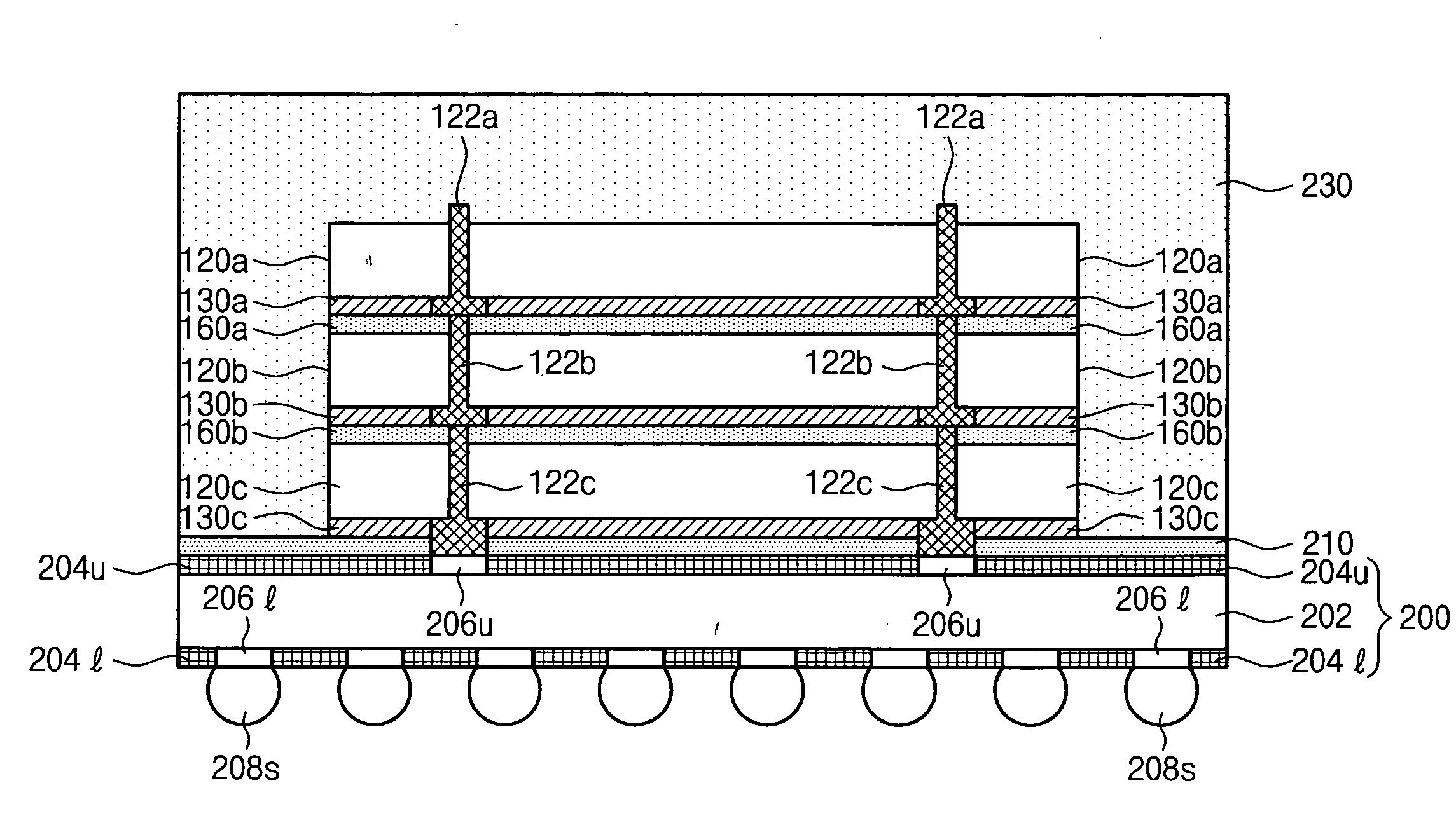
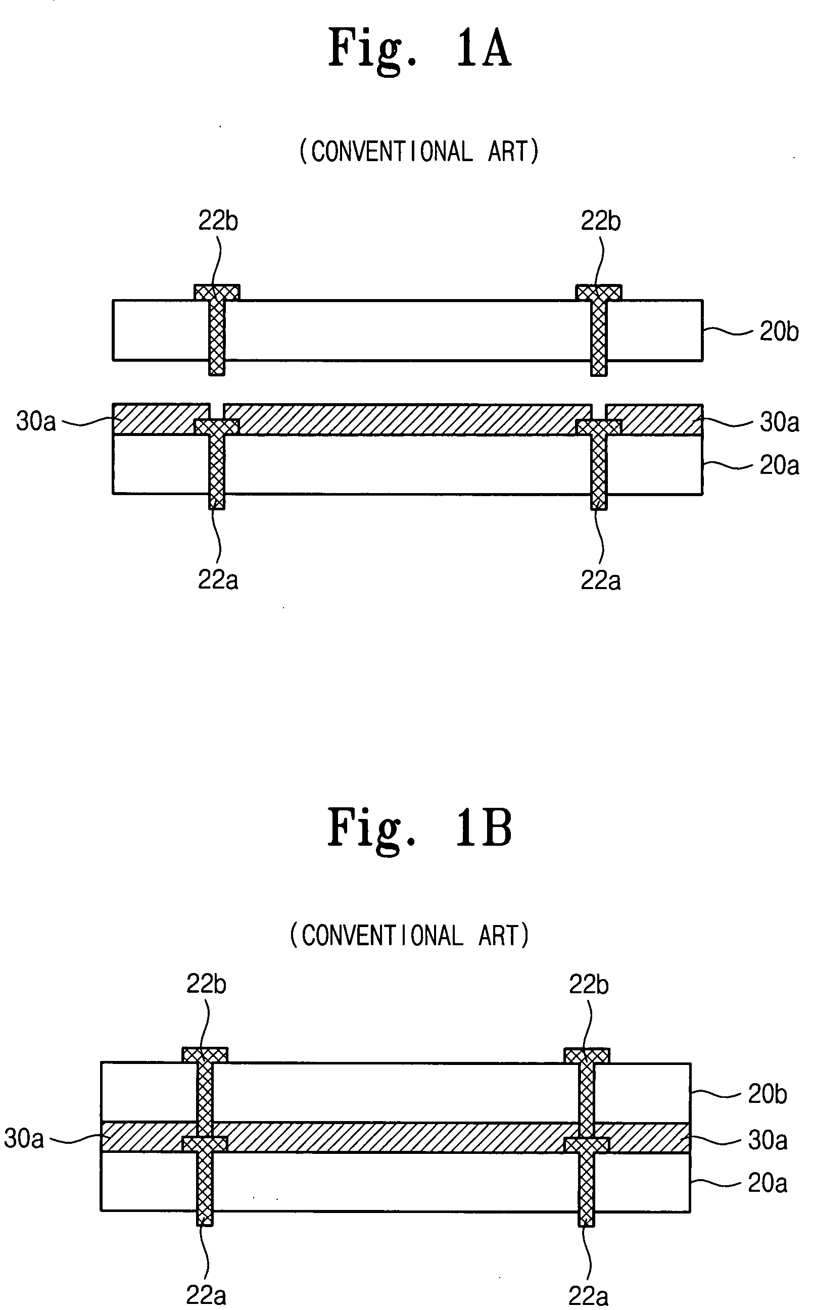
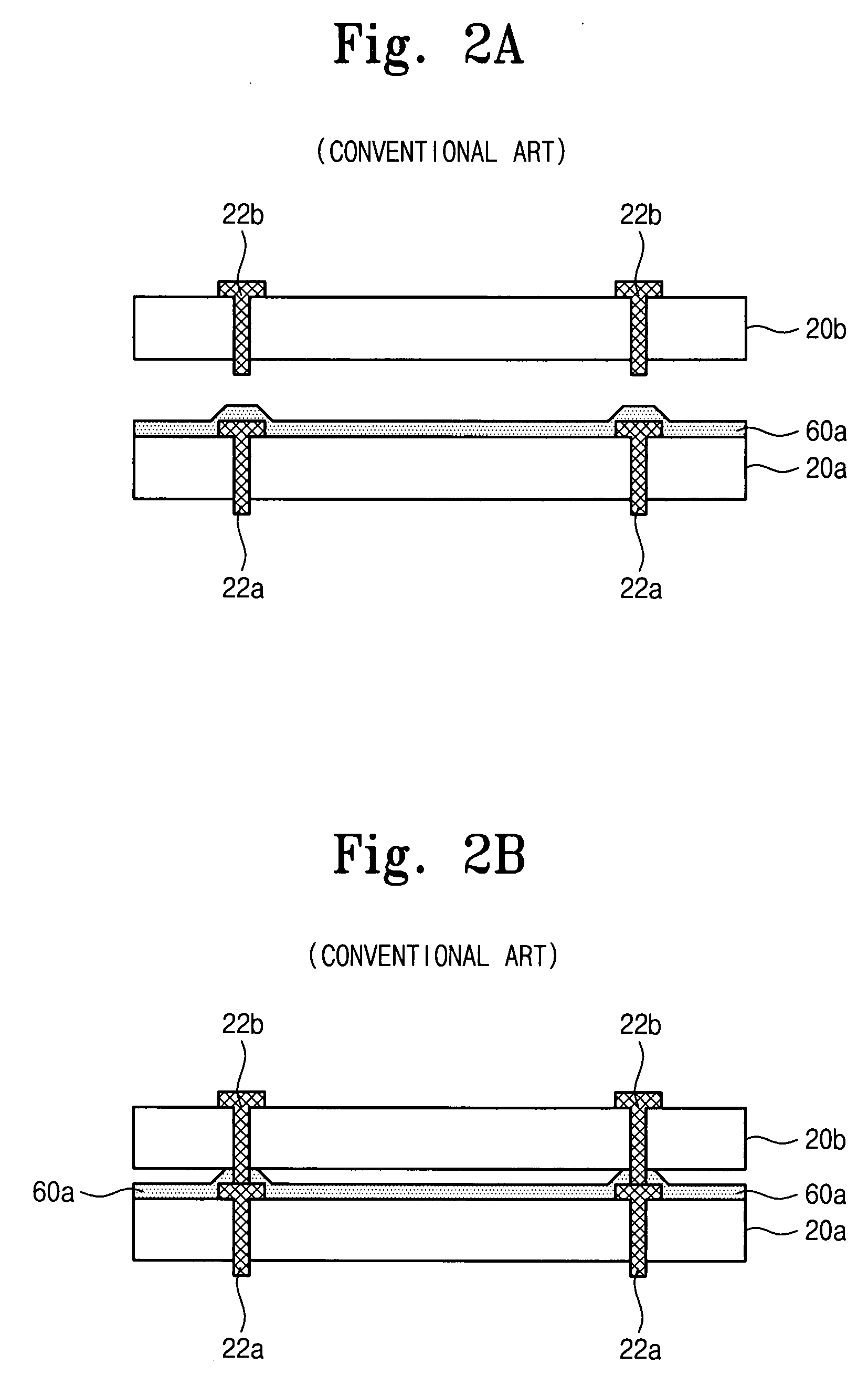
[0013]Example embodiments may relate to a semiconductor device package including a stacked structure of semiconductor devices, and methods of fabricating the same. Example embodiments may also relate to a semiconductor device package including a stacked structure of semiconductor devices, and methods for fabricating the same, using an adhesive structure including adhesives with different patterning and puncturing properties. An adhesive structure may include a first adhesive film having first patterning properties and first puncturing properties; and a second adhesive film on the first adhesive film, the second adhesive film having second patterning properties and second puncturing properties, wherein the first patterning properties are better than the second patterning properties, and the second puncturing properties are better than the first puncturing properties.

[0014]A method of stacking semiconductor devices may include preparing a plurality of semiconductor devices, each havin...


PUM


Abstract

A stacked structure of semiconductor devices may include a plurality of stacked semiconductor devices, each having an upper surface and a lower surface and one or more via electrodes protruding from the upper surface to the lower surface. The via-electrodes may have upper parts (heads) protruding from the upper surface and lower parts (ends) protruding from the lower surface. The stacked semiconductor devices may be electrically connected to each other through the via-electrodes. A first adhesive film (e.g., patternable material) and a second adhesive film (e.g. puncturable material) may be formed between the stacked semiconductor devices. The stacked structure of semiconductor devices may be mounted on the upper surface of a printed circuit board (PCB) having a mount-specific adhesive film to form a semiconductor device package. The mounted stacked structure and the upper surface of the PCB may be further covered with a molding material.

Description

PRIORITY STATEMENT[0001]This U.S. non-provisional patent application claims priority under 35 U.S.C. §119(a) to Korean Patent Application No. 10-2007-0004898, filed on Jan. 16, 2007 in the Korean Intellectual Property Office (KIPO), the entire contents of which are incorporated herein by reference.BACKGROUND[0002]1. Technical Field[0003]Example embodiments relate to a stacked structure of semiconductor devices, a semiconductor device package, and methods of fabricating the same.[0004]2. Description of Related Art[0005]Packaging technologies for integrated circuits (ICs) have been steadily improving to keep up with demands for miniaturization and / or mounting reliability. The demand for miniaturization has accelerated technical developments in the semiconductor chip packaging area, achieving a degree of miniaturization even as small as the actual size of a typical semiconductor chip. Mounting reliability may also be important to packaging, providing mounting efficiency and mechanical / ...

Claims


Application Information

Patent Timeline
IPC IPC(8): H01L23/02H01L21/00
CPCH01L21/6835H01L2224/0401H01L23/3128H01L23/481H01L24/12H01L24/33H01L24/83H01L24/90H01L25/0657H01L25/50H01L2221/68327H01L2221/68372H01L2224/0557H01L2224/13009H01L2224/13099H01L2224/16145H01L2224/32145H01L2224/73204H01L2224/81193H01L2224/83856H01L2225/06513H01L2225/06517H01L2225/06541H01L2924/01005H01L2924/01013H01L2924/01029H01L2924/0781H01L2924/14H01L24/32H01L2224/2919H01L2924/01006H01L2924/01033H01L2924/014H01L2924/0665H01L21/6836H01L2924/0002H01L2924/0132H01L2924/00H01L2224/05552H01L2924/181H01L2924/00012H01L23/12
Inventor KWON, YONG-CHAILEE, DONG-HOCHUNG, MYUNG-KEELEE, KANG-WOOKKANG, SUN-WONMA, KEUM-HEE
Owner SAMSUNG ELECTRONICS CO LTD
Why Eureka
Try Eureka