Display device

a display device and active matrix technology, applied in static indicating devices, instruments, optics, etc., can solve the problems of power consumption of the entire display device, the limitation of the power consumption reduction the inability to efficiently suppress so as to achieve the suppression of the effect of efficiently suppressing the power consumption of the signal line driver circuit and suppressing the power consumption of the entire display devi

Inactive Publication Date: 2008-07-17
SEMICON ENERGY LAB CO LTD
View PDF21 Cites 157 Cited by
  • Summary
  • Abstract
  • Description
  • Claims
  • Application Information

AI Technical Summary

Benefits of technology

[0079]Therefore, even when a plurality of groups each having a plurality of line periods where pieces of data correspond to each other exist, power consumption of the signal line driver circuit can be efficiently suppressed. Further, power consumption which is necessary for input of video signals to the signal line driver circuit can be suppressed, so that power consumption of the entire display device can be suppressed.
[0080]Further, in the display device of the present invention, by storing data of video signals corresponding to a plurality of line periods or a plurality of frame periods in a memory, a data comparison portion can compare data of a video signal corresponding to one line period with data of a video signal corresponding to a plurality of line periods other than one line period. Thus, comparison with not only data corresponding to adjacent line periods but also data corresponding to more line periods can be performed, so that power consumption of the signal line driver circuit can be efficiently suppressed.

Problems solved by technology

Thus, there is a problem in that power consumption of a signal line driver circuit and power consumption of the entire display device cannot efficiently suppressed even when the technique disclosed in Reference 1 is used.
In addition, there is also a problem in that there is limitation on reduction in power consumption of the entire display device by just devising leading of wirings as disclosed in Reference 2.

Method used


Image

  • Display device
  • Display device
  • Display device

Examples


embodiment mode 1

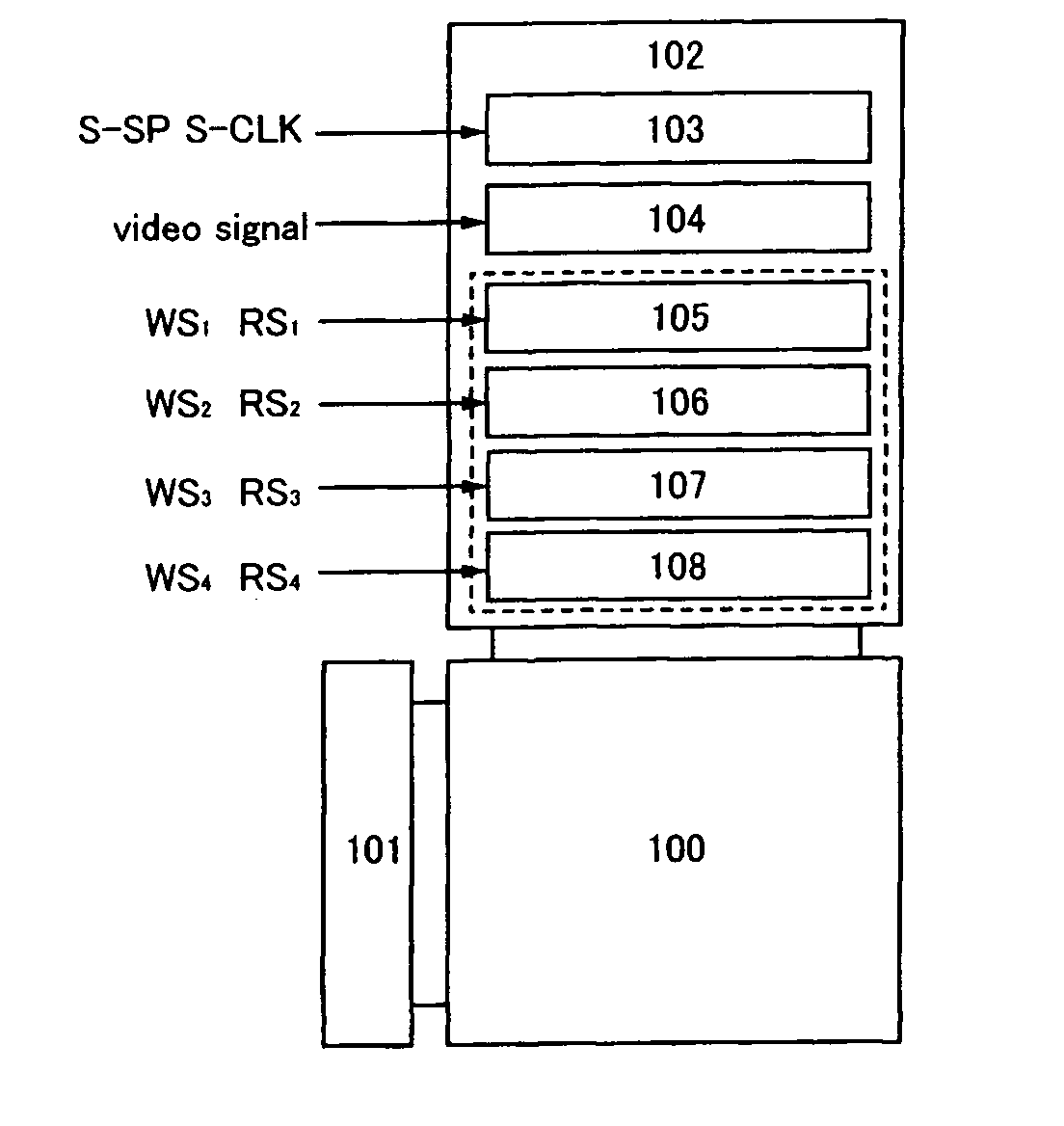
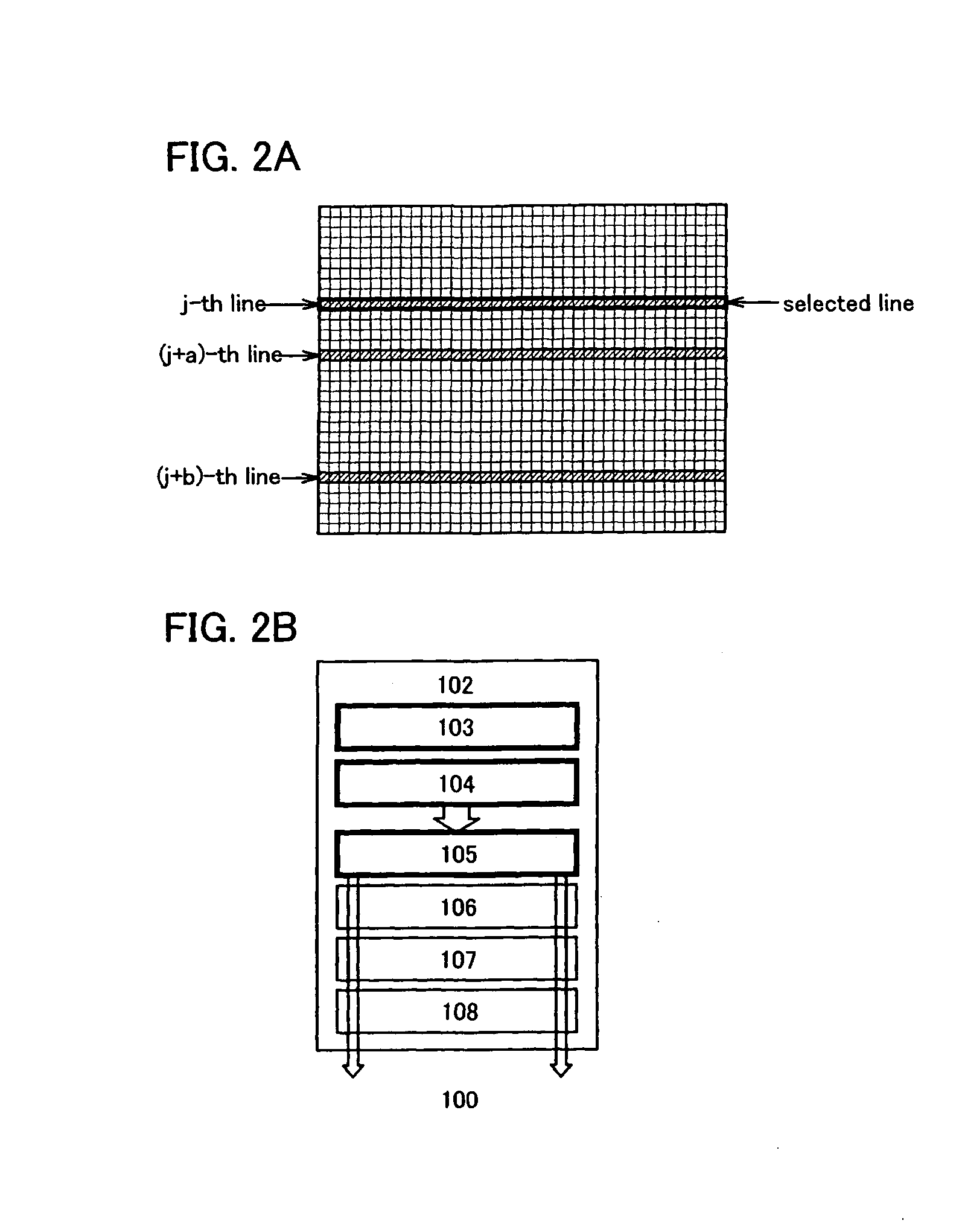
[0170]FIG. 1 is a block diagram of a display device of the present invention. The display device of the present invention includes a pixel portion 100 including a plurality of pixels, a scan line driver circuit 101 which can select a plurality of pixels in each line, and a signal line driver circuit 102 which controls input of a video signal to pixels in a selected line. The signal line driver circuit 102 includes at least a shift register 103, a sampling circuit 104, and a plurality of memory circuits. Each memory circuit includes a plurality of memory elements which can store data input to pixels for one line.

[0171]FIG. 1 shows an example in which a first latch 105, a second latch 106, a third latch 107, and a fourth latch 108 are used for the plurality of memory circuits. Note that the number of latches used in the display device of the present invention is not limited to four, and the number of latches may be two or three, or may be five or more.

[0172]Next, an operation of the s...

embodiment mode 2

[0211]FIG. 6 is a block diagram of a display device of the present invention. The display shown in FIG. 6 includes a memory for storing video signals and a data comparison portion 110 which compares video signals stored in the memory in corresponding line periods in addition to the display device shown in FIG. 1. FIG. 6 shows an example in which a RAM (random access memory) 111 and a RAM 112 are used as the memory for storing the video signals. For the RAMs 111 and 112, various RAMs such as an SDRAM (synchronous dynamic random access memory), a DRAM (dynamic random access memory), and an SRAM (static random access memory) can be used.

[0212]In addition, the display device of the present invention may include a control circuit 113 and a data format circuit 114 as shown in FIG. 6. A clock signal CLK and a signal which is used for reconstructing a screen in the pixel portion 100, such as a horizontal synchronization signal Hsync used for horizontal synchronization or a vertical synchron...

embodiment mode 3

[0240]In this embodiment mode, a structure of a scan line driver circuit included in a display device of the present invention is described. FIG. 11 shows a block diagram of a structure of the display device of the present invention as an example. FIG. 11 shows a more detailed structure of the scan line driver circuit 101 in the display device shown in FIG. 1. In FIG. 11, the scan line driver circuit 101 includes a shift register 121 and a buffer 122.

[0241]The start pulse signal G-SP and the clock signal G-CLK are input to the scan line driver circuit 101. The shift register 103 generates selection signals, pulses of which are sequentially shifted, in accordance with the start pulse signal G-SP and the clock signal G-CLK. The buffer 122 shapes waveforms of the generated selection signal or amplifies the generated selection signal and inputs the signal to the pixel portion 100. The selection signals are input to pixels in each line, and one line can be selected from a plurality of li...


PUM


Abstract

To provide an active matrix display device in which power consumption of a signal line driver circuit can be suppressed, so that power consumption of the entire memory can be suppressed. A plurality of memory circuits which can write data of a video signal input to a pixel in one line period and can hold the data are provided in a signal line driver circuit of a display device. Then, the data held in each memory circuit is input to a pixel of a corresponding line as a video signal. By providing two or more memory circuits in a driver circuit, pieces of data of video signals corresponding to two or more line periods can be concurrently held in the memory circuits.

Description

BACKGROUND OF THE INVENTION[0001]1. Field of the Invention[0002]The present invention relates to an active matrix display device in which input of a video signal to a pixel can be controlled by a driver circuit.[0003]2. Description of the Related Art[0004]In an active matrix display device, a switching element and a display element are provided in each of hundreds of thousand to millions of pixels arranged in matrix. Since application of voltage or supply of current to the display element is held to some extent by the switching element after a video signal is input to the pixel, the active matrix display device can be flexible on enlargement and high definition of a panel and has become the mainstream of future display devices.[0005]There are a scan line driver circuit and a signal line driver circuit as typical examples of a driver circuit included in the display device. A plurality of pixels in one line or a plurality of lines are selected at one time by a scan line driver circuit...

Claims


Application Information

Patent Timeline
Patent Type & Authority Applications(United States)
IPC IPC(8): G09G3/36
CPCG02F1/136213G09G3/20G09G3/3208G09G3/342G09G3/3648G09G2310/024G09G3/2085G09G2310/04G09G2310/061G09G2320/0252G09G2330/021G09G2340/16G09G2310/027G09G3/30G09G3/36G09G5/39G09G2360/12
Inventor YOSHIDA, YASUNORI
Owner SEMICON ENERGY LAB CO LTD
Why Eureka
Try Eureka