Uniaxial strain relaxation of biaxial-strained thin films using ion implantation

a thin film, uniaxial strain technology, applied in the direction of semiconductor devices, basic electric elements, electrical apparatus, etc., can solve the problems of increasing the difficulty of sustraining the advancement by conventional mosfet miniaturization, inability to scale, and inability to achieve optimal biaxial compressive strain configuration,

Inactive Publication Date: 2008-07-17
IBM CORP
View PDF14 Cites 10 Cited by
  • Summary
  • Abstract
  • Description
  • Claims
  • Application Information

AI Technical Summary

Benefits of technology

[0010]The present invention relates to a method for forming uniaxial strain in a continuous biaxially strained semiconductor film by uniaxially relaxing that film without patterning the biaxially strained film. In one aspect of the present invention, a patterned structure (such as an ion implant block mask or a field effect transistor) is formed atop the continuous biaxially strained film. Ion implantation is then performed to form damaged regions and subsequent relaxation within unprotected portions of the biaxially strained semiconductor film. The portion of the biaxially strained semiconductor film covered by the patterned structure relaxes at the boundary of the damaged regions inward in a manner that is similar to that described in the prior art.

Problems solved by technology

However, as the device scale reaches the nanometer regime and below, it is increasingly difficult to sustrain the advancement by conventional MOSFET miniaturization.
Therefore, methods for improving performance, without scaling, have become increasingly critical.
However, the biaxial compressive strain is not an optimal configuration since the compressive strain in the transverse direction would degrade pFET performance.
It is clear from FIGS. 2A-2B that this prior art approach relies on the patterning of the strained film, which would impose requirements on the device geometry and introduce complexity to device design.

Method used


Image

  • Uniaxial strain relaxation of biaxial-strained thin films using ion implantation
  • Uniaxial strain relaxation of biaxial-strained thin films using ion implantation
  • Uniaxial strain relaxation of biaxial-strained thin films using ion implantation

Examples


Embodiment Construction

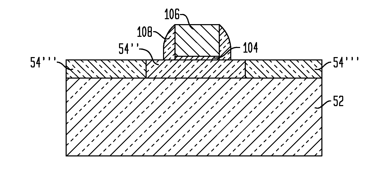
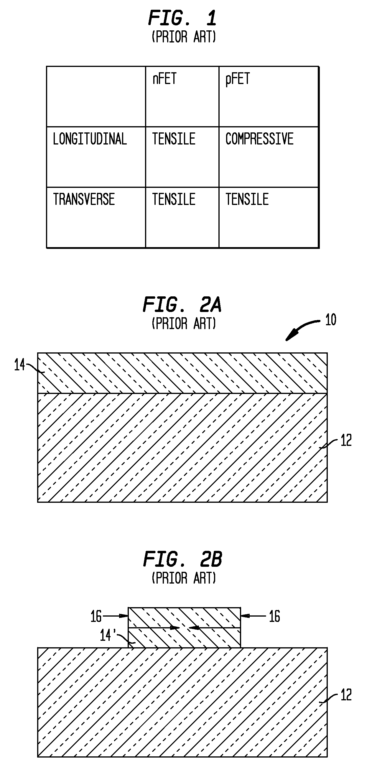
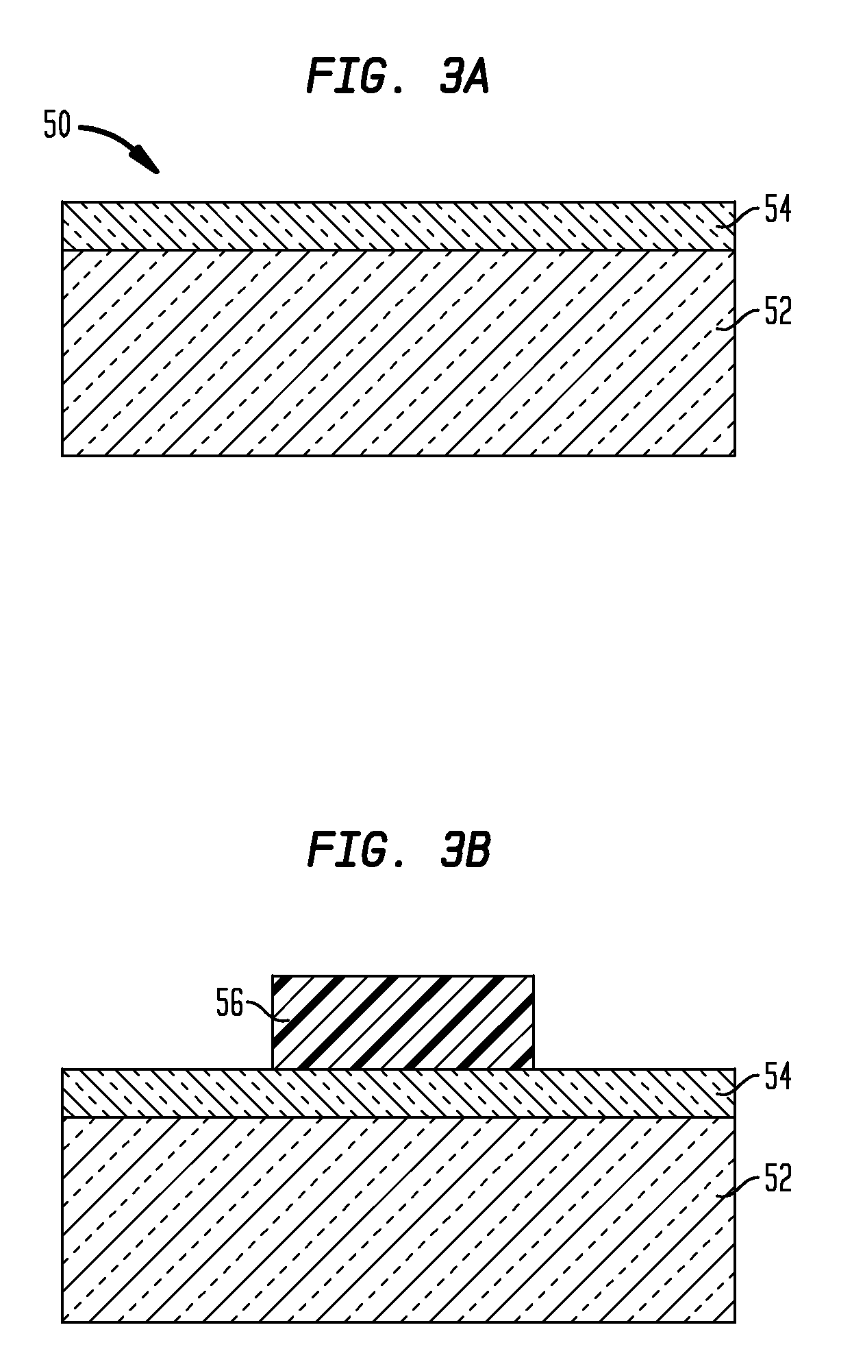
[0023]The present invention, which provides a method of achieving uniaxial strain relaxation of an originally biaxially strained semiconductor film without subjecting the film to patterning prior to uniaxial strain relaxation, will now be described in greater detail by referring to the following discussion and drawings that accompany the present application. It is noted that the drawings of the present application are provided for illustrative purposes and, as such, they are not drawn to scale.

[0024]In the following description, numerous specific details are set forth, such as particular structures, components, materials, dimensions, processing steps and techniques, in order to provide a thorough understanding of the present invention. However, it will be appreciated by one of ordinary skill in the art that the invention may be practiced with viable alternative process options without these specific details. In other instances, well-known structures or processing steps have not been...


PUM


Abstract

A method for achieving uniaxial strain on originally biaxial-strained thin films after uniaxial strain relaxation induced by ion implantation is provided. The biaxial-strained thin film receives ion implantation after being covered by a patterned implant block structure. The strain in the uncovered region is relaxed by ion implantation, which induces the lateral strain relaxation in the covered region. When the implant block structure is narrow (dimension is comparable to the film thickness), the original biaxial strain will relax uniaxially in the lateral direction.

Description

FIELD OF THE INVENTION[0001]The present invention relates to strained semiconductor materials, and more particularly to a method of forming uniaxial strain for enhanced electron and hole mobilities.BACKGROUND OF THE INVENTION[0002]The conventional miniaturization of metal oxide semiconductor field effect transistors (MOSFETs) has been the driving force in the technology advancement for the semiconductor industry for more than three decades. However, as the device scale reaches the nanometer regime and below, it is increasingly difficult to sustrain the advancement by conventional MOSFET miniaturization. Therefore, methods for improving performance, without scaling, have become increasingly critical. One general approach for doing this is to increase carrier (electron and / or hole) mobilities in MOSFETs. Use of stress on MOSFETs has proved to be an effective way to enhance carrier mobilities in the transistor channel.[0003]As shown in FIG. 1, different semiconductor devices need diffe...

Claims


Application Information

Patent Timeline
Patent Type & Authority Applications(United States)
IPC IPC(8): H01L21/425
CPCH01L21/26506H01L29/7848H01L29/78H01L21/823807Y10S438/938
Inventor REN, ZHIBINSAENGER, KATHERINE L.YIN, HAIZHOU
Owner IBM CORP
Why Eureka
Try Eureka