Elevated pocket pixels, imaging devices and systems including the same and method of forming the same

a technology of imaging devices and pocket pixels, applied in the direction of diodes, semiconductor devices, radiation controlled devices, etc., can solve the problems of electron/carrier recombination, impede “complete” charge transference, and difficulty in transferring all of the photogenerated charge from the photosensor to the floating diffusion region

Active Publication Date: 2008-07-24
MICRON TECH INC
View PDF10 Cites 83 Cited by
  • Summary
  • Abstract
  • Description
  • Claims
  • Application Information

AI Technical Summary

Problems solved by technology

CMOS image sensors may have difficulty transferring all of the photogenerated charge from the photosensor to the floating diffusion region.
One problem with transferring charge occurs when the n-type silicon layer of the photosensor is located close to the surface; this causes electron/carrier recombination due to surface defects.
Another obstacle hindering “complete” charge transference includes potential barriers that exist at the gate of the transfer transistor.
Additionally, known CMOS image sensors provide only approximately a fifty percent fill factor, meaning only half of the pixel cell is utilized in converting light to c

Method used


Image

  • Elevated pocket pixels, imaging devices and systems including the same and method of forming the same
  • Elevated pocket pixels, imaging devices and systems including the same and method of forming the same
  • Elevated pocket pixels, imaging devices and systems including the same and method of forming the same

Examples


Embodiment Construction

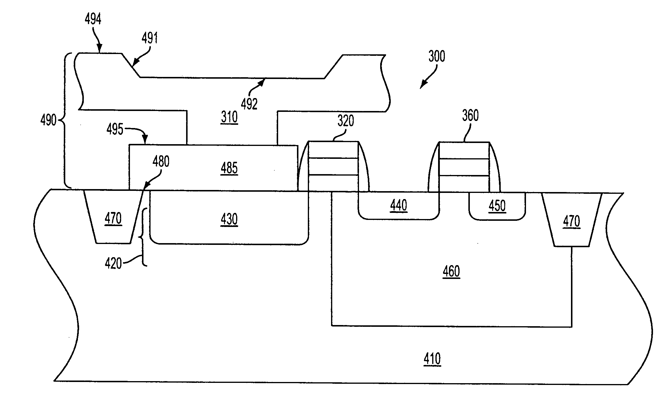
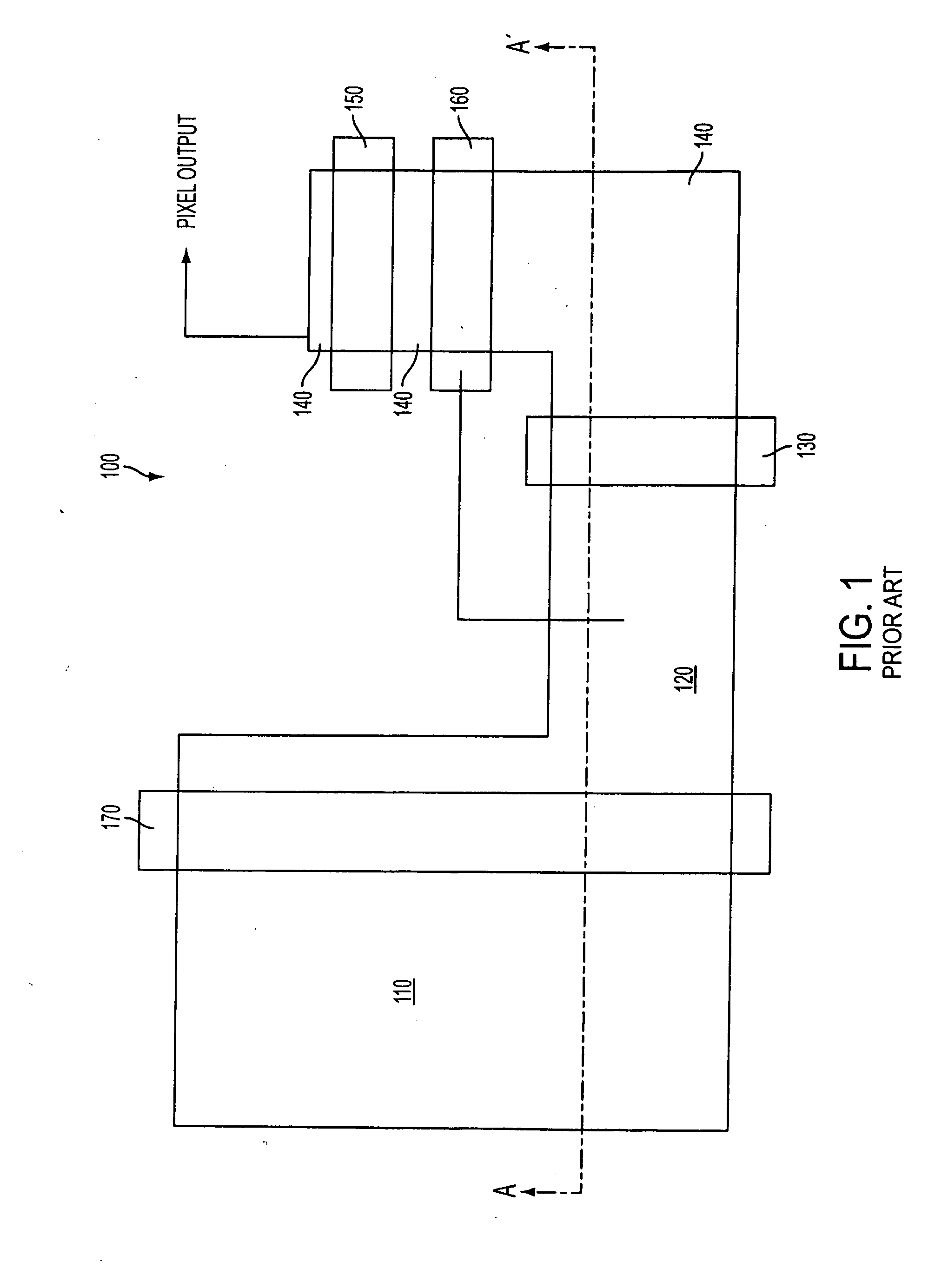
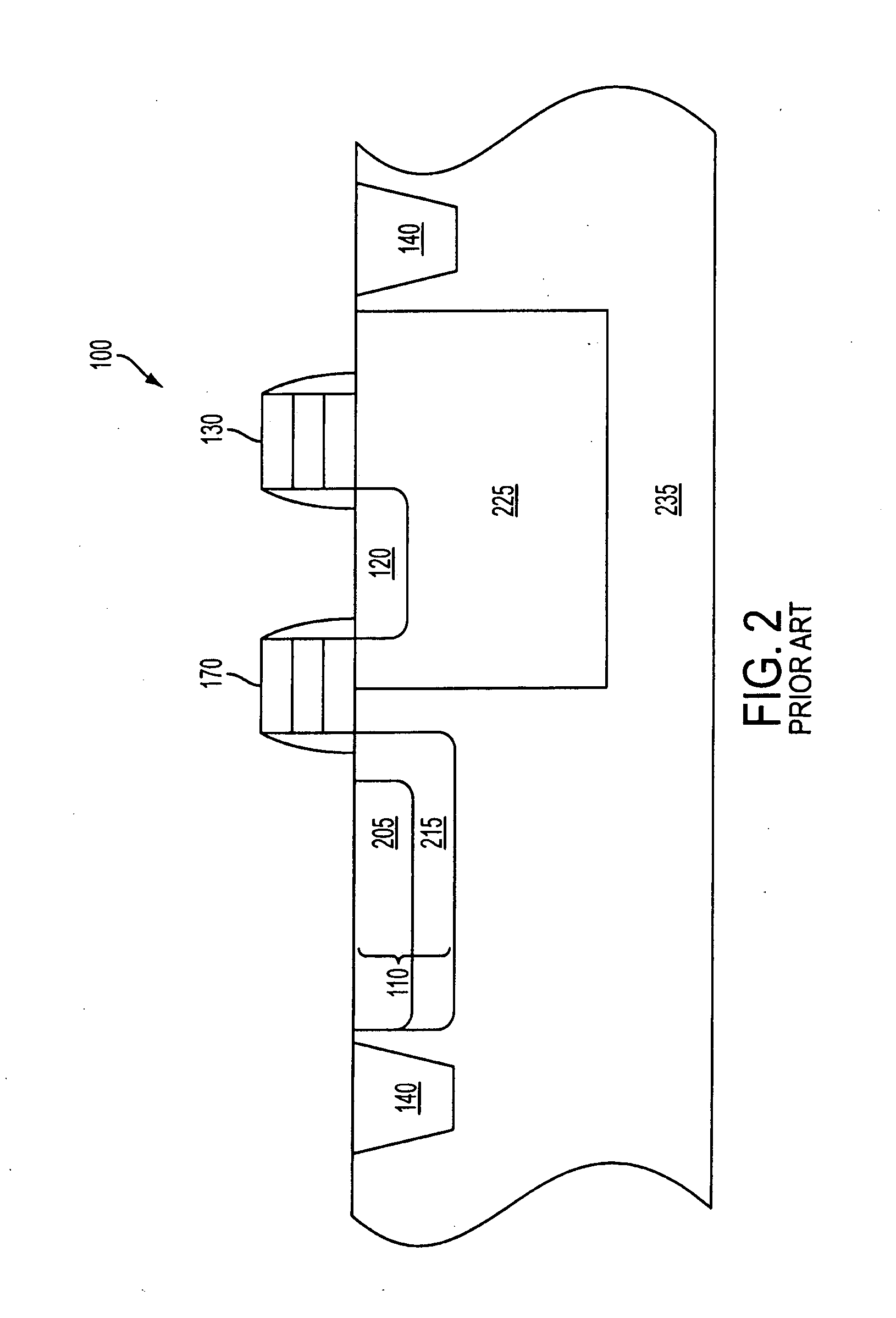
[0040]In the following detailed description, reference is made to the accompanying drawings which form a part hereof and illustrate embodiments that may be practiced. It should be understood that like reference numerals represent like elements throughout the drawings. These embodiments are described in sufficient detail to enable those skilled in the art to practice them, and it is to be understood that other embodiments may be utilized, and that structural, logical and electrical changes may be made.

[0041]The term “substrate” is to be understood as including silicon-on-insulator (SOI) or silicon-on-sapphire (SOS) technology, doped and undoped semiconductors, epitaxial layers of silicon supported by a base semiconductor foundation, and other semiconductor structures. Furthermore, when reference is made to a “substrate” in the following description, previous process steps may have been utilized to form regions or junctions in the base semiconductor structure or foundation. In additio...


PUM


Abstract

An elevated photosensor for image sensors and methods of forming the photosensor. The photosensor may have light sensors having indentation features including, but not limited to, v-shaped, u-shaped, or other shaped features. Light sensors having such an indentation feature can redirect incident light that is not absorbed by one portion of the photosensor to another portion of the photosensor for additional absorption. In addition, the elevated photosensors reduce the size of the pixel cells while reducing leakage, image lag, and barrier problems.

Description

CROSS REFERENCE TO RELATED APPLICATIONS[0001]This application is related to application Ser. No. 11 / 300,378, filed on Dec. 15, 2005, the disclosure of which is hereby incorporated by reference herein in its entirety.BACKGROUND OF THE INVENTION[0002]Solid state image sensors are increasingly being used in a wide variety of imaging applications as low cost imaging devices. One such image sensor is a CMOS image sensor. A CMOS image sensor includes a focal plane array of pixel cells. Each cell includes a photosensor, photogate, photoconductor, or photodiode having an associated charge accumulation region within a substrate for accumulating photo-generated charge. Each pixel cell may include a transistor for transferring charge from the charge accumulation region to a floating diffusion region, and a transistor for resetting the floating diffusion region to a predetermined charge level. The pixel cell may also include a source follower transistor for receiving and amplifying charge from ...

Claims


Application Information

Patent Timeline
IPC IPC(8): H01L31/0232H01L31/18
CPCH01L27/14621H01L27/14627H01L27/14632H01L27/14643H01L27/14685H01L27/14687H01L31/1804H01L31/028H01L31/02162H01L27/14692H01L27/14605H01L31/03762H01L31/035281H01L27/14689H01L27/14603H01L27/14601H01L27/146H01L27/14647H01L27/14607H01L27/14645H01L31/0352H01L31/022408H01L31/0288
Inventor AKRAM, SALMAN
Owner MICRON TECH INC
Why Eureka
Try Eureka