Semiconductor device

a technology of semiconductor devices and mother boards, applied in semiconductor devices, semiconductor/solid-state device details, electrical apparatus, etc., can solve the problems of affecting the performance of the mother board, affecting the effect of heat release, and most of the heat generated in the integrated circuit is intensively transferred to the mother board, so as to reduce the adverse effect of the mother board due to heat, effectively promote heat loss, and reduce the adverse effect of the mother board

Inactive Publication Date: 2008-07-24
SEIKO EPSON CORP
View PDF5 Cites 1 Cited by
  • Summary
  • Abstract
  • Description
  • Claims
  • Application Information

AI Technical Summary

Benefits of technology

[0006]An advantage of the present invention is to reduce adverse effect on a mother board by using a resin layer.
[0007](1) A semiconductor device according to the invention includes: a semiconductor substrate having an integrated circuit formed thereon and an electrode electrically coupled to the integrated circuit; a passivation film formed on a surface of the semiconductor substrate, the surface having the electrode formed thereon; a first metal layer formed so as to come into contact with the passivation film; a resin layer formed on the first metal layer; a wiring formed so as to be electrically coupled to the electrode and reach an upper surface of the resin layer; and a second metal layer formed so as to be in contact with the first metal layer and reach the upper surface of the resin layer. According to the invention, the first metal layer comes into contact with the passivation film so as to transfer heat to the second metal layer, thereby making it possible to effectively promote heat loss. Accordingly, when the semiconductor device is mounted on a mother board, adverse effect on the mother board due to heat can be reduced.
[0008](2) In this case, the first metal layer may come, at its entire side opposed to the passivation film, into contact with the passivation film.
[0009](3) In this case, the semiconductor device may further include a second resin layer formed on the passivation film, and the first metal layer may include a portion contacting the passivation film and a portion positioned on the second resin layer.
[0010](4) In this case, the first metal layer may come, only at its end, into contact with the passivation film.
[0011](5) In this case, the first metal layer may come, at least a part of its end, into contact with the passivation film, and a region except the end of the first metal layer may include the portion contacting the passivation film and the portion positioned on the second resin layer.

Problems solved by technology

However, when the surface (active surface), on which an integrated circuit is formed, is covered by the resin layer, heat release performance is deteriorated.
Accordingly, when the semiconductor device is mounted on a mother board, most of heat generated in the integrated circuit is disadvantageously transferred to the mother board intensively on the external terminal.
Therefore, there arises an adverse effect due to heat on the mother board.

Method used


Image

  • Semiconductor device
  • Semiconductor device
  • Semiconductor device

Examples


first embodiment

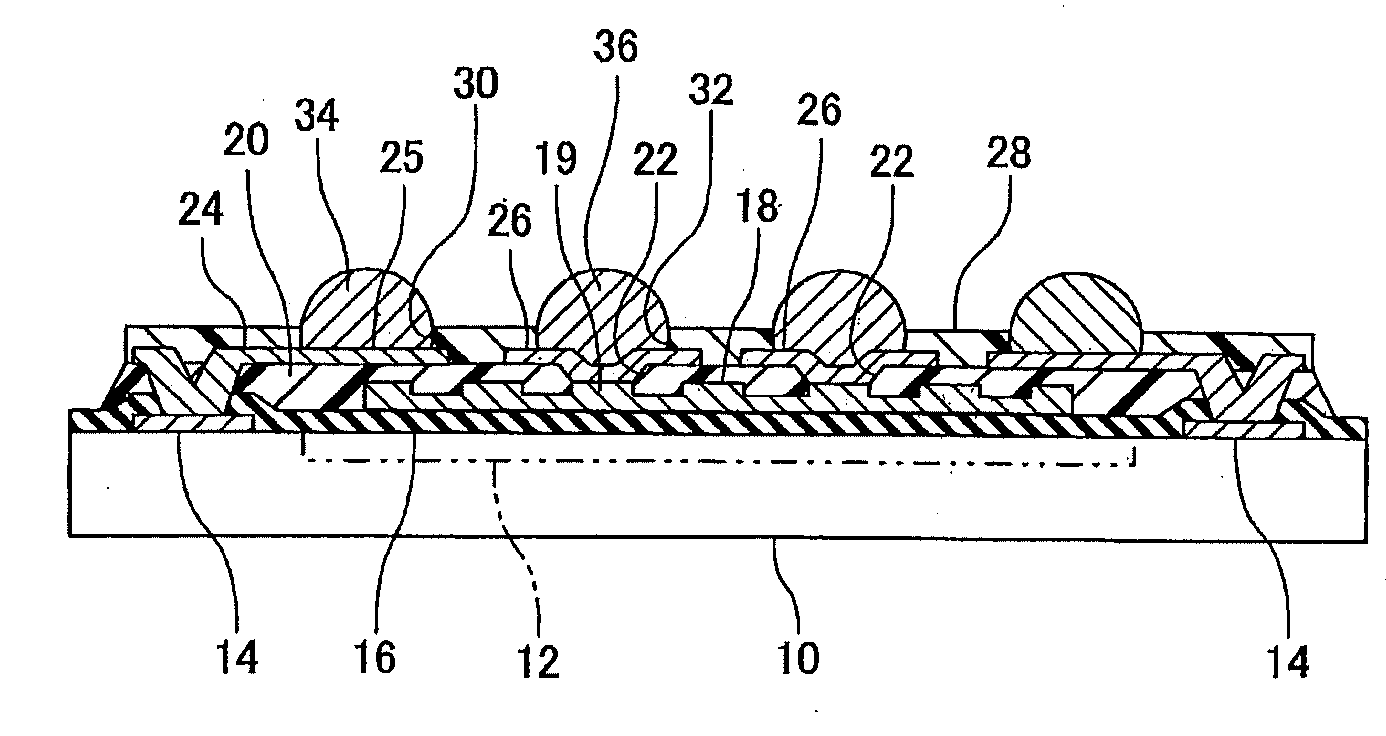
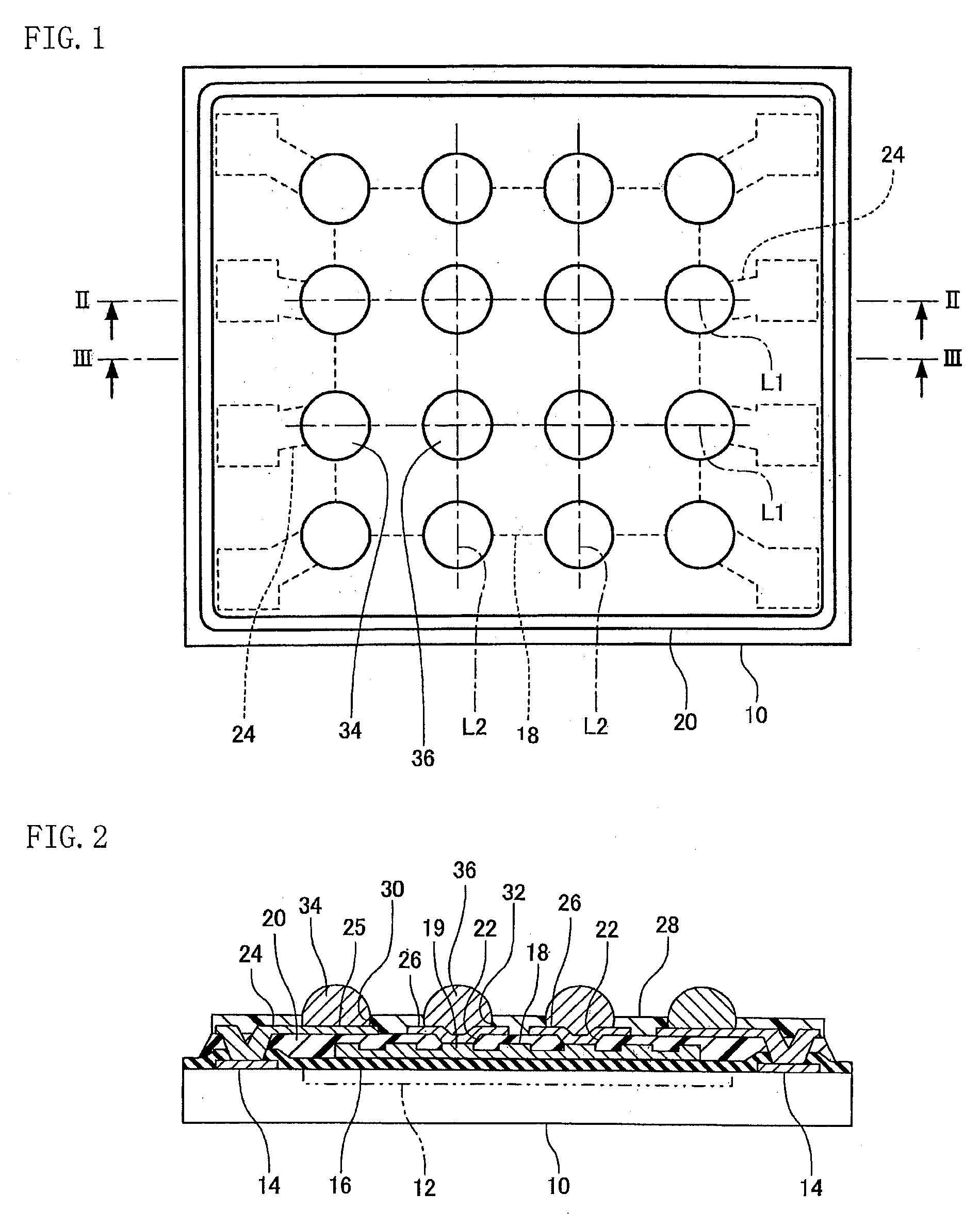
[0024]FIG. 1 is a view showing a semiconductor device according to a first embodiment of the invention. FIG. 2 is a sectional view taken along the line II-II of the semiconductor device shown in FIG. 1. FIG. 3 is a sectional view taken along the line III-III of the semiconductor device shown in FIG. 1.

[0025]The semiconductor device includes a semiconductor substrate 10. As finished product, the semiconductor substrate 10 is a semiconductor chip, as shown in FIG. 1, while the semiconductor substrate 10 is a semiconductor wafer as interim product when in a fabrication process. Provided in the semiconductor substrate 10 is an integrated circuit 12 (there are one integrated circuit 12 in the case of the semiconductor chip shown in FIG. 1 and a plurality of integrated circuits 12 in the case of the semiconductor wafer). The integrated circuit 12 is to be worked in one surface of the semiconductor substrate 10. Provided in each integrated circuit 12 and is a plurality of electrodes 14, wh...

second embodiment

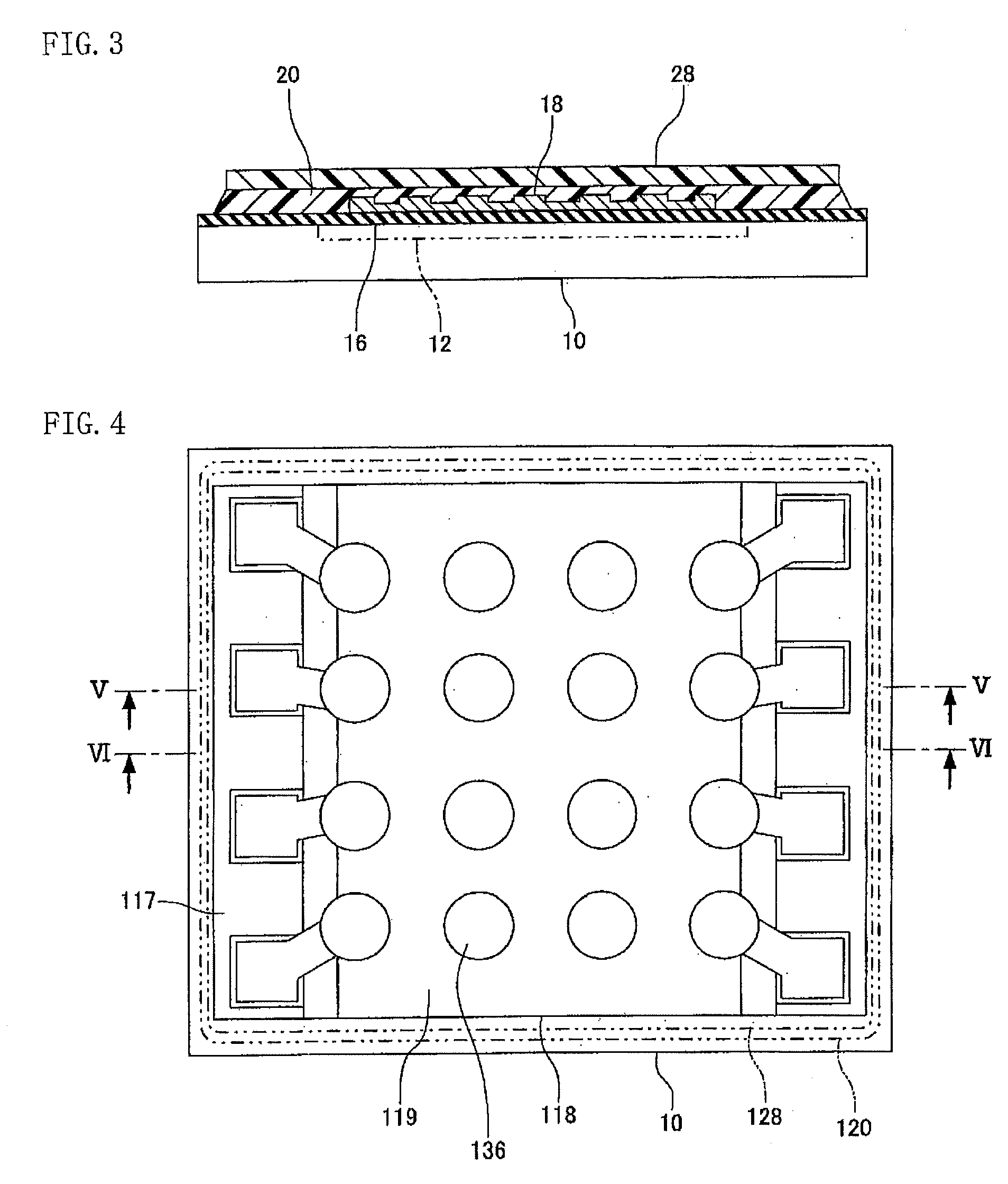
[0035]FIG. 4 is a view showing a semiconductor device according to a second embodiment of the invention. FIG. 5 is a sectional view taken along with the line V-V of the semiconductor device shown in FIG. 4. FIG. 6 is a sectional view taken along with the line VI-VI of the semiconductor device shown in FIG. 4.

[0036]According to this embodiment of the invention, a second resin layer 100 is provided on the passivation film 16. The second resin layer 100 can be formed by using photolithography with the use of photosensitive resin. It is also possible to form the second resin layer 100 by using thermosetting resin. The second resin layer 100 can be inclined at its lateral surface 102 so that the lateral surface 102 makes an acute angle with the bottom surface of the second resin layer. The inclination of the lateral surface 102 can be made by thermal contraction of thermosetting resin precursor.

[0037]The first metal layer 18 includes a portion 117 contacting the passivation film 16 and a...

third embodiment

[0039]FIG. 7 is a view showing a semiconductor device according to a third embodiment of the invention. FIG. 8 is a sectional view taken along with the line VIII-VIII of the semiconductor device shown in FIG. 7. FIG. 9 is a sectional view taken along with the line IX-IX of the semiconductor device shown in FIG. 7.

[0040]According to this embodiment of the invention, provided on the passivation film 16 is a second resin layer 200. The second resin layer 200 may be, as shown in FIG. 8 and FIG. 9, divided into a plurality of portions, have just a through-hole and be not separated, or have a projection, which does not extending therethrough. In all the cases, the upper surface of the second resin layer 200 is made uneven.

[0041]A first metal layer 218 includes portions 215, 219 contacting the passivation film 16 and a portion 217 positioned on the second resin layer 200. The first resin layer 218 is in contact with the passivation film 16 at a part of a end 215 (at the entire peripheral p...


PUM


Abstract

A semiconductor device includes: a semiconductor substrate having an integrated circuit formed thereon and an electrode electrically coupled to the integrated circuit; a passivation film formed on a surface of the semiconductor substrate, the surface having the electrode formed thereon; a first metal layer formed so as to come into contact with the passivation film; a resin layer formed on the first metal layer; a wiring formed so as to be electrically coupled to the electrode and reach an upper surface of the resin layer; and a second metal layer formed so as to be in contact with the first metal layer and reach the upper surface of the resin layer.

Description

[0001]The entire disclosure of Japanese Patent Application No. 2007-010573, filed Jan. 19, 2007 is expressly incorporated by reference herein.BACKGROUND OF THE INVENTION[0002]1. Technical Field[0003]The present invention relates to a semiconductor device.[0004]2. Related Art[0005]Recently, a packaging called wafer-level CSP is being developed, in which a wiring is formed on a semiconductor chip so as to form an external terminal (see JP-A-2003-282790). Provided under the wiring is a resin layer so that stress generated at the wiring is distributed and absorbed. However, when the surface (active surface), on which an integrated circuit is formed, is covered by the resin layer, heat release performance is deteriorated. Further, the wiring can hardly dissipate heat, because the wiring is covered by a solder mask except a land, on which a solder ball is to be laid. Accordingly, when the semiconductor device is mounted on a mother board, most of heat generated in the integrated circuit i...

Claims


Application Information

Patent Timeline
Patent Type & Authority Applications(United States)
IPC IPC(8): H01L23/52
CPCH01L23/3114H01L2224/0401H01L24/02H01L24/13H01L24/14H01L2224/0233H01L2224/02331H01L2224/02351H01L2224/0236H01L2224/02377H01L2224/02381H01L2224/024H01L2224/13022H01L2224/131H01L2224/14131H01L2924/014H01L2924/14H01L23/525H01L2924/01033H01L2924/01006H01L2924/01023H01L2224/02125H01L2224/02235H01L2224/05548H01L2224/05569H01L2224/13024H01L2924/0001H01L2224/02
Inventor HANAOKA, TERUNAO
Owner SEIKO EPSON CORP
Why Eureka
Try Eureka