Phase adjusting device and related art thereof
- Summary
- Abstract
- Description
- Claims
- Application Information
AI Technical Summary
Benefits of technology
Problems solved by technology
Method used
Image
Examples
first embodiment
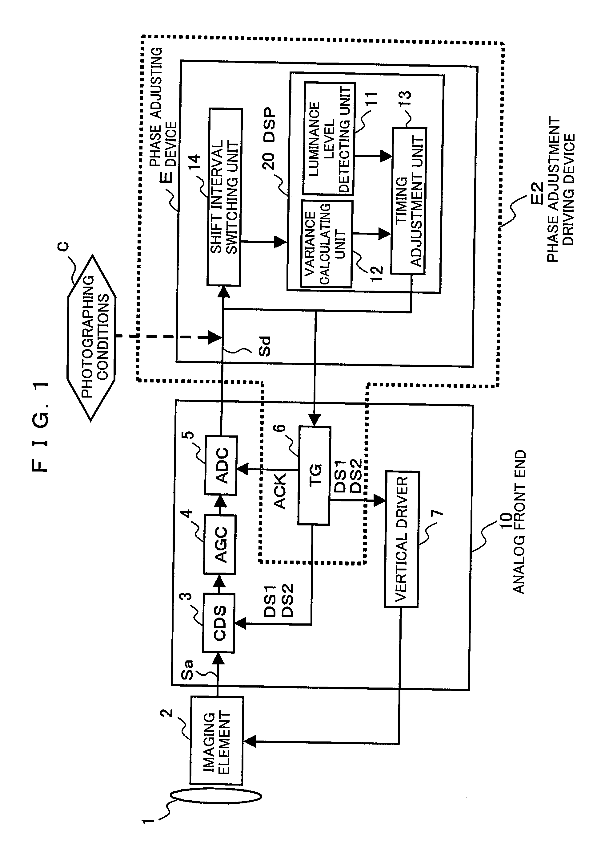
[0056]FIG. 1 is a block diagram showing an overall configuration of a digital camera according to a first embodiment of the present invention. The digital camera of the present embodiment includes an optical lens 1 for collecting a subject image on an imaging element 2, the imaging element 2 (CCD is hereinafter described by way of example) for imaging the subject image collected by the optical lens 1, an analog front end 10 for performing a predetermined process on an analog imaged signal Sa output from the imaging element 2 to convert the analog imaged signal Sa to a digital imaged signal Sd, and a DSP (Digital signal Processor) 20 for performing a predetermined process (color correction, YC process, etc.) on the digital imaged signal Sd output from the analog front end 10 to generate an image signal. The imaging element 2 includes a plurality of pixels, which plurality of pixels include an effective pixel region used for imaging the subject and an OB (Optical Black) pixel region a...
second embodiment
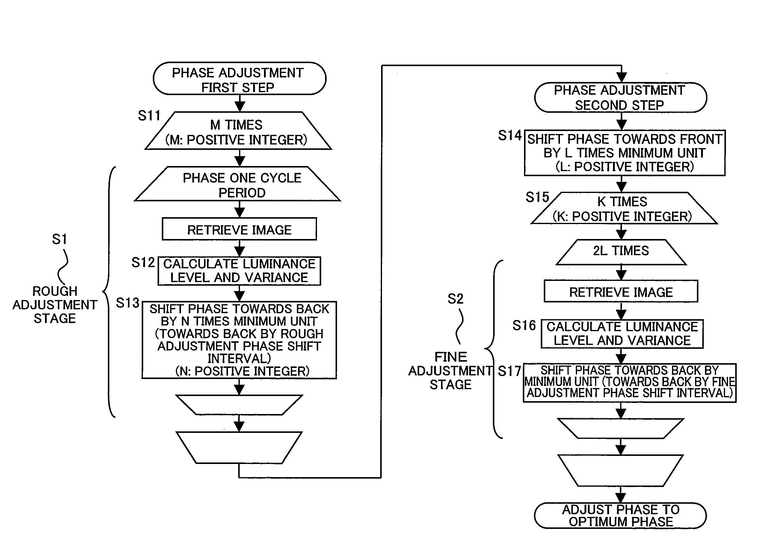
[0096]The second embodiment of the present invention further enhances the precision of the phase adjustment of the AD clock signal ACK. FIG. 10 is a view showing a timing chart of a signal component used in the phase adjustment of the AD clock signal ACK. As N and L used in FIG. 4, N=3 and L=1.
[0097]In the rough adjustment stage S1, the phase of the AD clock signal ACK is shifted at the rough adjustment phase shift interval (interval that is three times the minimum unit interval of the phase shift) T3 in such a way as A1 to A4 of P41 with the phases of the reference sample pulse DS1 and the peak sample pulse DS2 fixed at the first imaging phases to detect the phase at which the variance W3 becomes a minimum in the variance calculation (S12). If there are two variance-value sub-portions 31 and 32 at which the variance W3 becomes small as shown in FIG. 10, the luminance level at each phase detected with respect to both phases (A2 and A4 of P41) at which the variance W3 in each of the ...
PUM
 Abstract
Description
Claims
Application Information


