Pattern Inspection Apparatus and Semiconductor Inspection System

a technology of semiconductor inspection and pattern, applied in the direction of photomechanical equipment, instruments, optics, etc., can solve the problems of difficulty in distinguishing such a defective part of the circuit pattern, erroneous detection of defects, and unclear shape suitable for comparison with the circuit pattern, etc., to achieve accurate and efficient detection of defects

Active Publication Date: 2008-07-24
HITACHI HIGH-TECH CORP
View PDF1 Cites 24 Cited by
  • Summary
  • Abstract
  • Description
  • Claims
  • Application Information

AI Technical Summary

Benefits of technology

[0011]In view of the aforementioned circumstances, it is an object of the present invention to provide a pattern inspection apparatus which solves the problems of the conventional techniques, and which is capable of detecting a defect accurately and efficiently. Moreover, the present invention also provides a semiconductor inspection system using such a pattern inspection apparatus.
[0019]According to the present invention, it is possible to provide a pattern inspection apparatus capable of detecting defects accurately and efficiently in a pattern of a semiconductor device by comparing a non-linear part of a captured image with an angular part of design data.

Problems solved by technology

Accordingly, there is a problem that even a part having no defect in view of an electrical characteristic may be detected as a defect by using the conventional method in which difference values are simply obtained from the design data and the shape of the pattern to be inspected, and in which then a position having a difference value equal to or more than a fixed value is detected as a defective position.
Furthermore, there is difficulty in distinguishing such a defective part of the circuit pattern by using the differential information.
Even with the method disclosed in JP-A No. 2005-277395, erroneous detection of defects may probably occur in a case where the positioning of both design data and the image is not precisely performed, a case where the actual pattern largely expands or contracts as compared with the pattern of design data, and a case where an unintended pattern is included in an image area estimated from design data.
However, the shape appropriate for comparison with the circuit pattern is sometimes unclear before inspection and erroneous detection of defects may occur due to an error in comparison between the reference pattern and the circuit pattern on the wafer.

Method used


Image

  • Pattern Inspection Apparatus and Semiconductor Inspection System
  • Pattern Inspection Apparatus and Semiconductor Inspection System
  • Pattern Inspection Apparatus and Semiconductor Inspection System

Examples


Embodiment Construction

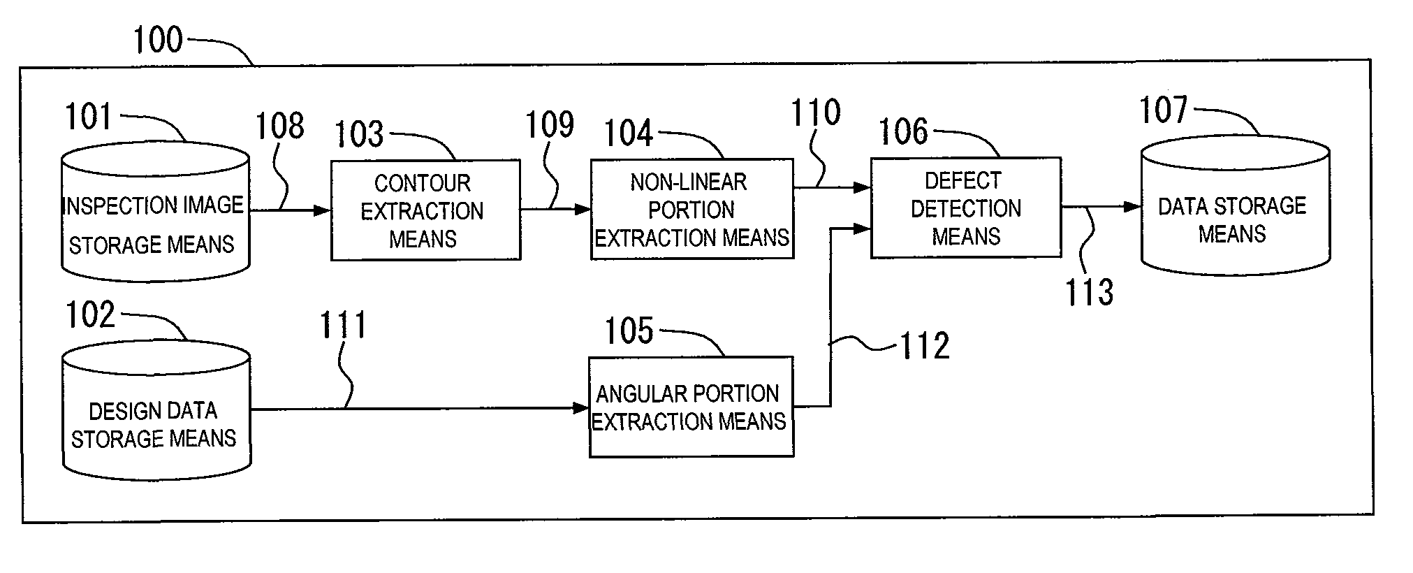
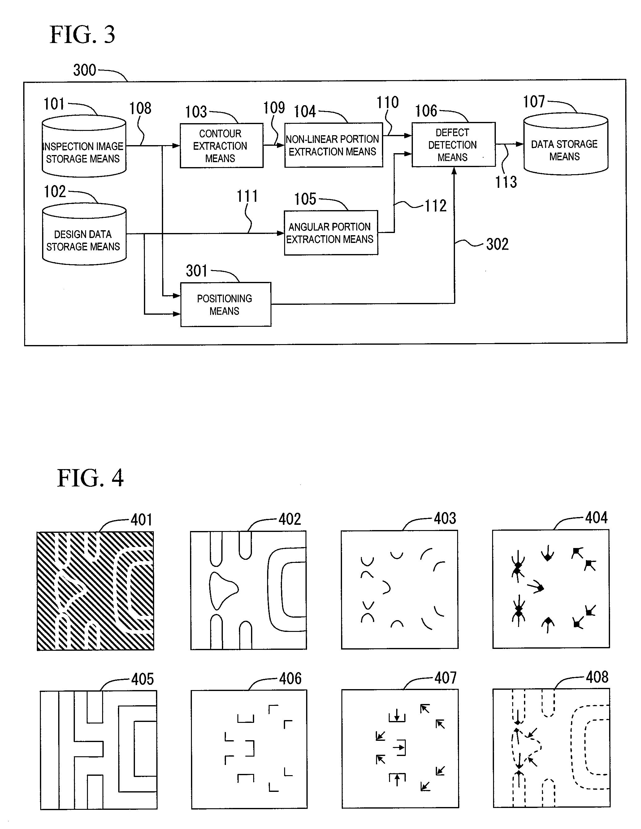
[0034]In the present invention, as shown in FIG. 4, a captured image 401 of a circuit pattern and design data 405 of the circuit pattern are compared with each other to detect a defective part 408 of the circuit pattern included in the image 401. The present invention uses the fact in which detective parts of a pattern such as cutting, short-circuit and distortion of the pattern, and adhesion of foreign material are formed as a non-linear pattern in the same manner as an angular part such as a line end and a corner of the pattern. In the present invention, a non-linear part 403 of the circuit pattern is detected from the captured image 401 of the circuit pattern, and an angular part 406 of the pattern such as a line end and a corner is detected from design data 405. Then, the presence or absence of corresponding points between the non-linear part 403 extracted from the image 401 and the angular part 406 extracted from the design data 405 is inspected, thereby detecting the defective...


PUM


Abstract

There is provided a pattern inspection apparatus that is capable of detecting a defect accurately and efficiently to inspect a pattern of a semiconductor device. The pattern inspection apparatus includes: a contour extraction means for extracting contour data of a pattern from a captured image of the semiconductor device; a non-linear part extraction means for extracting a non-linear part from the contour data; an angular part extraction means for extracting an angular part of a pattern from design data of the semiconductor device; and a defect detection section that compares a position of the non-linear part extracted by the non-linear part extraction section with a position of the angular part extracted by the angular part extraction section so as to detect a position of a defective part of a pattern.

Description

BACKGROUND OF THE INVENTION[0001]1. Field of the Invention[0002]The present invention relates to a pattern inspection apparatus that inspects a pattern formed on a wafer by using an image of a semiconductor device and design data of the semiconductor device. The present invention also relates to a semiconductor inspection system composed of an electron microscope and a computer that operates as the pattern inspection apparatus.[0003]2. Description of the Related Art[0004]In semiconductor devices in recent years, miniaturization and multilayering have been advanced and the logic has become complicated, causing extreme difficulties in the manufacture thereof. As a result, defects attributable to the manufacture process tend to occur frequently, and it is accordingly important to detect the defects efficiently and correctly and to specify a problem of the manufacture process.[0005]The defects attributable to the manufacture process include deformation, cutting, short-circuit of the pat...

Claims


Application Information

Patent Timeline
Patent Type & Authority Applications(United States)
IPC IPC(8): G06K9/00
CPCG06T7/001G06T7/0004
Inventor TOYODA, YASUTAKASUTANI, TAKUMICHIMATSUOKA, RYOICHINAYA, HIDEMITSU
Owner HITACHI HIGH-TECH CORP
Why Eureka
Try Eureka