Package substrate, method of fabricating the same and chip package

a technology of packaging substrate and chip package, which is applied in the direction of resist details, printed circuit aspects, conductive pattern formation, etc., can solve the problem of reducing manufacturing yield, excessive process temperature, and the requirement of high density of substrate bump b>130/b>, so as to improve the reliability of the chip package structure, high integration, and high distribution density

Inactive Publication Date: 2008-07-31
ADVANCED SEMICON ENG INC
View PDF12 Cites 111 Cited by
  • Summary
  • Abstract
  • Description
  • Claims
  • Application Information

AI Technical Summary

Benefits of technology

[0010]The present invention is directed to a package substrate on which substrate bumps of high distribution density are disposed. The package substrate is applicable in a chip package technology requiring high integration. Moreover, the package substrate is conducive to improving the reliability of a chip package structure.

Problems solved by technology

Since the package substrate is usually a polymer substrate made of organic materials and is not of high heat resistance, it is not allowed to have an excessively-high process temperature at which a reflow process is carried out for bonding the chip to the polymer substrate.
If substrate bumps 130 are formed by performing the screen-printing method, the high density requirement of the substrate bump 130 cannot be satisfied due to limitations on the fabrication of a printing screen and printing solder materials.
Moreover, the overly-short pitches d1 between the bonding pads 110 easily give rise to erroneous bridging of substrate bumps 130, thus reducing the manufacturing yield.
Therefore, the reliability of the chip package structure is impaired.

Method used


Image

  • Package substrate, method of fabricating the same and chip package
  • Package substrate, method of fabricating the same and chip package
  • Package substrate, method of fabricating the same and chip package

Examples


first embodiment

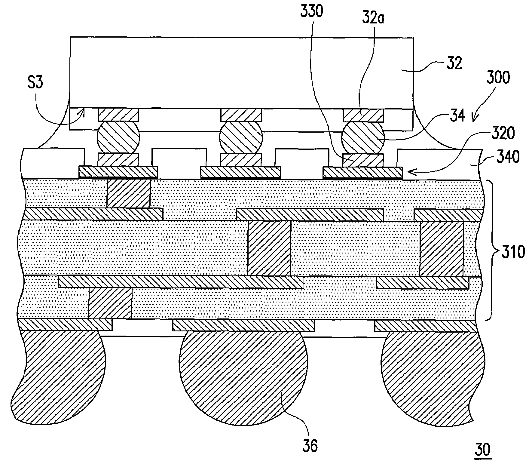
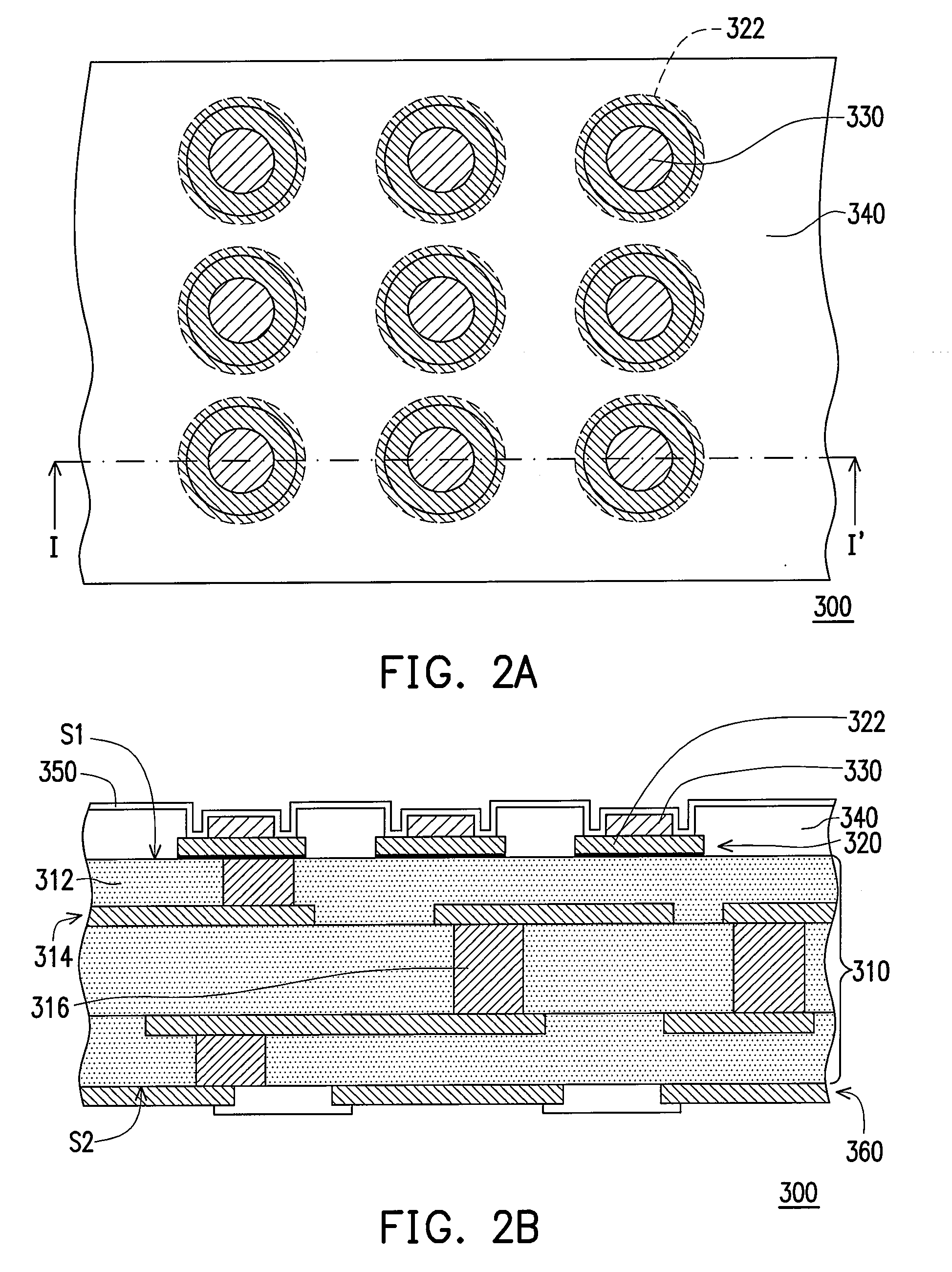
[0045]FIG. 2A is a schematic top view of a package substrate according to a first embodiment of the present invention. FIG. 2B is a schematic cross-sectional view illustrating the package substrate depicted in FIG. 2A along a sectional line I-I′. Referring to FIGS. 2A and 2B, a package substrate 300 provided by the first embodiment includes a base layer 310, a surface circuit layer 320, a plurality of conductive bumps 330, and a patterned solder mask layer 340. The surface circuit layer 320 having a plurality of bonding pads 322 is disposed on a surface S1 of the base layer 310. The conductive bumps 330 are disposed on the bonding pads 322 individually to serve as substrate bumps. In addition, the patterned solder mask layer 340 is disposed on the surface S1 of the base layer 310 and outside a corresponding region occupied by the conductive bumps 330, so as to expose the conductive bumps 330.

[0046]In the first embodiment, the conductive bumps 330 include a plurality of metal posts, ...

second embodiment

[0058]FIG. 5A is a schematic top view of a package substrate according to a second embodiment of the present invention. FIG. 5B is a schematic cross-sectional view illustrating the package substrate depicted in FIG. 5A along a sectional line II-II′. Referring to FIGS. 5A and 5B, the difference between a package substrate 400 provided by the second embodiment and the package substrate 300 discussed in the first embodiment lies in that a patterned solder mask layer 440 of the package substrate 400 in the second embodiment is further disposed outside the corresponding region occupied by bonding pads 422, so as to expose the bonding pads 422 and conductive bumps 430 disposed thereon.

third embodiment

[0059]FIG. 6A is a schematic top view of a package substrate according to a third embodiment of the present invention. FIG. 6B is a schematic cross-sectional view illustrating the package substrate depicted in FIG. 6A along a sectional line III-III′. Referring to FIGS. 6A and 6B, the difference between a package substrate 500 provided by the present embodiment and the package substrates 300 and 400 discussed in the previous embodiments lies in that a solder mask layer 540 exposes the entire region of bonding pads 522 and conductive bumps 530 (a region bonding to the chip). In detail, the package substrate 500 has a chip bonding region A on a base layer 510. The bonding pads 522 and the conductive bumps 530 disposed thereon are arranged in arrays in the chip bonding region A, while the patterned solder mask layer 540 exposes the chip bonding region A. The design of the solder mask layer according to the second embodiment and the third embodiment more or less contributes to reducing t...


PUM

PropertyMeasurementUnit
conductiveaaaaaaaaaa
contact densityaaaaaaaaaa
electrical performanceaaaaaaaaaa

Abstract

A package substrate, including a base layer, a surface circuit layer, a plurality of conductive bumps, and a patterned solder mask layer, is provided. The surface circuit layer having a plurality of bonding pads is disposed on a surface of the base layer. The conductive bumps are disposed on the bonding pads individually. The patterned solder mask layer is disposed on the surface of the base layer and outside a corresponding region occupied by the conductive bumps, so as to expose the conductive bumps. In addition, a method of fabricating the package substrate and a chip package structure employing the package substrate are also provided.

Description

CROSS-REFERENCE TO RELATED APPLICATION[0001]This application claims the priority benefit of Taiwan application serial no. 96102832, filed on Jan. 25, 2007. The entirety of the above-mentioned patent application is hereby incorporated by reference herein and made a part of this specification.BACKGROUND OF THE INVENTION[0002]1. Field of the Invention[0003]The present invention relates to a circuit board, a method of fabricating the same, and a semiconductor device. More particularly, the present invention relates to a package substrate, a method of fabricating the same, and a chip package structure.[0004]2. Description of Related Art[0005]In flip-chip bonding technology commonly seen in semiconductor packaging industry, a chip bump is often fabricated on each chip pad, which is formed on an active surface of a wafer, such that the chip bump serves as an intermedium for electrically connecting a chip, which is formed by sawing the wafer, to a carrier. Since the flip-chip bonding techno...

Claims


Application Information

Patent Timeline
Patent Type & Authority Applications(United States)
IPC IPC(8): H01L23/488H05K3/00H05K1/00
CPCH01L23/49816Y10T29/49155H01L2224/16H01L2924/01079H01L2924/15311H05K1/111H05K3/108H05K3/243H05K3/282H05K3/3452H05K3/4007H05K2201/0367H05K2201/0989H05K2203/0574H01L23/49838H01L2224/16237H01L2224/05573H01L2224/05568H01L2924/00014H01L2224/0554H01L2224/05599H01L2224/0555H01L2224/0556
Inventor LIAO, GUO-CHENG
Owner ADVANCED SEMICON ENG INC
Why Eureka
Try Eureka