Ultra-fine pitch probe card structure

Inactive Publication Date: 2008-07-31
TAIWAN SEMICON MFG CO LTD
View PDF20 Cites 15 Cited by
  • Summary
  • Abstract
  • Description
  • Claims
  • Application Information

AI Technical Summary

Benefits of technology

[0011]An advantage of embodiments of the present invention is that a smaller co

Problems solved by technology

Unfortunately, this type of probe card 100 is limited due to the fact that the contact pads are limited to the peripheral of the semiconductor device to be tested, and it cannot reach contact pads located in the central areas of the devices.
U

Method used


Image

  • Ultra-fine pitch probe card structure
  • Ultra-fine pitch probe card structure
  • Ultra-fine pitch probe card structure

Examples


Embodiment Construction

[0020]The making and using of the embodiments are discussed in detail below. It should be appreciated, however, that the present invention provides many applicable inventive concepts that can be embodied in a wide variety of specific contexts. The specific embodiments discussed are merely illustrative of specific ways to make and use the invention, and do not limit the scope of the invention.

[0021]The present invention will be described with respect to embodiments in a specific context, namely a probe card. The invention may also be applied, however, to other non-permanent electrical connections.

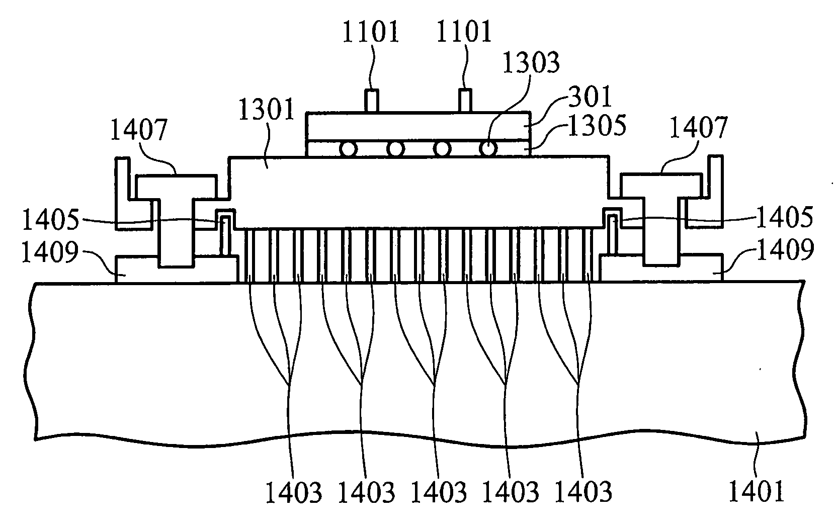
[0022]With reference now to FIG. 3, there is shown a substrate 301 with a via 303 of conductive material formed within the substrate 301. The substrate 301 comprises a semiconductor material such as silicon, germanium, silicon germanium, or combinations thereof. The substrate 301 is initially between about 400 μm to about 725 μm, with a preferred thickness of about 500 μm.

[0023]The via 303 m...


PUM


Abstract

A system and a method of testing a semiconductor die is provided. An embodiment comprises a plurality of tips that each comprise a substrate with a conductive via, a first dielectric layer with vias connected to the conductive via, a second dielectric layer with vias over the first dielectric layer, and a metal layer over the second dielectric layer. Additional dielectric layers with vias may be used. This tip is electrically connected to a redistribution line that routes signals between the tip to electrical connections on a space transformation layer. The space transformation layer is electrically connected to a printed circuit board using, for example, a spring loaded connection such as a pogo pin. The space transformation layer is aligned onto the printed circuit board by a series of guidance mechanisms such as guide pins or smooth fixtures, and the planarity of the tips is adjusted by adjusting the screws.

Description

[0001]This application claims the benefit of U.S. Provisional Application No. 60,898,461, filed on Jan. 31, 2007, entitled “Ultra-Fine Pitch Probe Card Structure,” which application is hereby incorporated herein by reference.TECHNICAL FIELD[0002]The present invention relates generally to a system for testing semiconductor devices and, more particularly, to a system and method for forming a probe card with an ultra-fine pitch.BACKGROUND[0003]In the manufacturing of integrated circuits and other semiconductor devices, the circuits and devices must be tested in order to ensure that a functional device has been manufactured. These tests are usually performed by contacting a test probe card to the relevant areas of the semiconductor device, and performing one or more functional tests. Two main types of probe cards are currently used to make these connections.[0004]FIG. 1 illustrates a plan view of one type of probe card 100 that is used to test a semiconductor device (not shown). This pr...

Claims


Application Information

Patent Timeline
IPC IPC(8): G01R1/073G01R31/00
CPCG01R1/07378G01R1/07342
Inventor CHENG, HSU MINGCHAO, CLINTONCHANG, FA-YUANWU, HUA-SHU
Owner TAIWAN SEMICON MFG CO LTD
Why Eureka
Try Eureka