Semiconductor package and lidar transmission unit

a technology of semiconductor and transmission unit, applied in the field of semiconductor package, can solve the problems of high cost and high cost of semiconductor fabrication, and achieve the effects of saving costs, reducing manufacturing costs, and reducing manufacturing costs

Inactive Publication Date: 2020-11-12
IBEO AUTOMOTIVE SYST
View PDF0 Cites 0 Cited by
  • Summary
  • Abstract
  • Description
  • Claims
  • Application Information

AI Technical Summary

Benefits of technology

[0005]The invention is based on the idea of using, instead of contacting by bond wires, contacting via a so-called interposer, wherein the interposer makes contact with the surface-emitting laser and the corresponding driver circuits via so-called solder bumps. Since such interposers can also be fabricated in a semiconductor fabrication process, these can have a very small pitch of the contacts which makes it possible to use surface-emitting lasers with a narrow array spacing. As a result, whilst the resolution of the surface-emitting laser remains the same, the laser can be reduced in size so that inexpensive laser arrays are possible.

Problems solved by technology

In the case of an at least required resolution of the surface-emitting laser, a minimum size of the laser is thus predefined which can result in high costs in the semiconductor fabrication since both the semiconductor surface per se and also the error rate, which increases the rejects in the case of larger semiconductor components results in higher costs.

Method used


Image

  • Semiconductor package and lidar transmission unit
  • Semiconductor package and lidar transmission unit
  • Semiconductor package and lidar transmission unit

Examples


Embodiment Construction

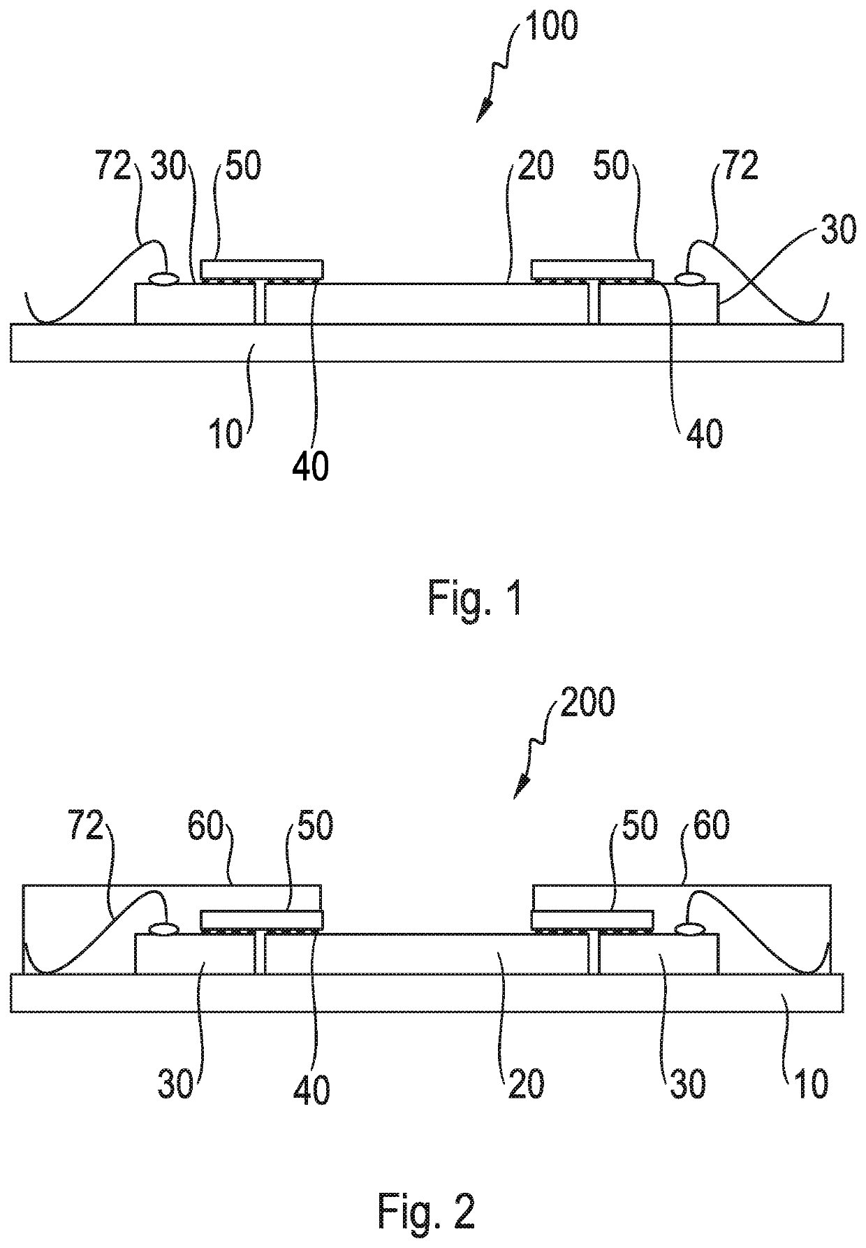
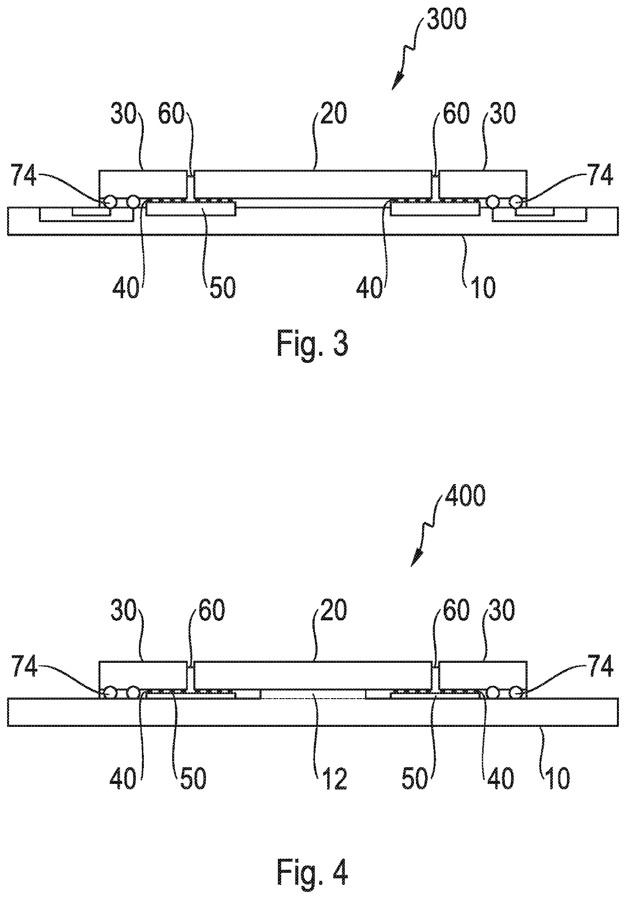
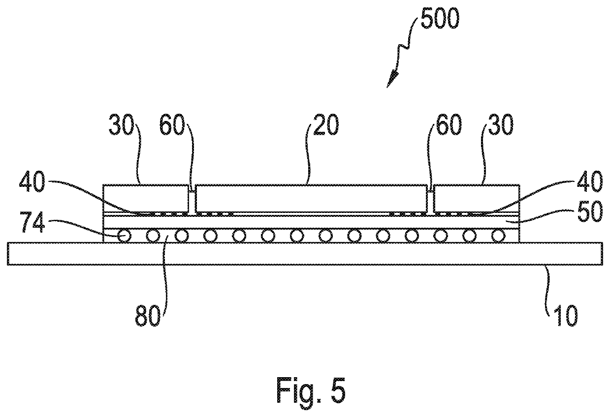
[0026]Exemplary embodiments are now described in detail with reference to the appended drawings which show some exemplary embodiments. In the following description of the appended figures which merely show some exemplary embodiments, the same reference numbers can designate the same or comparable components. Furthermore, summarizing reference numbers can be used for components and objects which occur multiple times in one exemplary embodiment or in one drawing but are described jointly with regard to one or several features. In this case, a vertical extension or a vertical arrangement is defined orthogonally to a front side of the package substrate and a lateral extension or a lateral arrangement is defined parallel to the front side of the package substrate.

[0027]FIG. 1 shows an exemplary embodiment of a semiconductor package. The semiconductor package 100 comprises a package substrate 10, a surface-emitting laser 20, two driver circuits 30 for the surface-emitting laser 20, a conn...


PUM

PropertyMeasurementUnit
diameteraaaaaaaaaa
diameteraaaaaaaaaa
diametersaaaaaaaaaa

Abstract

The present invention relates to a semiconductor package and to a LIDAR transmitting unit including such a semiconductor package. The semiconductor package has a surface-emitting laser, at least one driver circuit for the surface-emitting laser, a connecting structure and at least one interposer. The connecting structure includes a plurality of solder bumps. The surface-emitting laser is electrically connected to the at least one driver circuit via the at least one interposer and the connecting structure.

Description

FIELD OF THE INVENTION[0001]The present invention relates to a semiconductor package, more precisely to a semiconductor package comprising a surface-emitting laser, at least one driver circuit for the surface-emitting laser and at least one interposer as well as to a LIDAR transmitting unit comprising such a semiconductor package.BACKGROUND OF INVENTION[0002]In laser array arrangements, such as for LIDAR applications (Light Detection and Ranging, light-based detection and distance measurement), surface-emitting lasers, so-called VCSEL (Vertical-Cavity Surface-Emitting Laser, surface-emitting laser with a vertical resonator) are frequently used. These surface-emitting lasers, together with corresponding driver circuits, are arranged on a semiconductor package. In this case, it is usual that the electrical contacting between the driver circuits and the surface-emitting laser is made by means of bond wires.[0003]In some applications such as in the automobile area, such bond wires have ...

Claims


Application Information

Patent Timeline
Patent Type & Authority Applications(United States)
IPC IPC(8): H01S5/183H01L23/00G01S7/484H01L23/488
CPCH01S5/183G01S7/484H01L24/14H01L23/488H01S5/0261H01S5/18G01S7/4815G01S7/481H01L2224/16227H01L2224/1703H01L2924/15192H01L2924/15311H01L2224/73204H01L2224/32225H01L2224/92125H01L2924/18161H01L2224/131H01L2224/48227H01L2224/73265H01L2224/48465H01L2224/73207H01L2224/73253H01L2924/1815H01L2224/48091H01L24/13H01L24/16H01L24/17H01L24/32H01L24/48H01L24/73H01L24/92H01S5/02234H01S5/02325H01S5/0237H01S5/02345H01L2924/014H01L2924/00014H01L2924/00012H01L2224/16225H01L2924/00H01L23/48H01L24/10H01L24/42H01L24/97G01S7/4808G01S7/4813G01S7/4861
Inventor HAKSPIEL, STEFAN
Owner IBEO AUTOMOTIVE SYST
Why Eureka
Try Eureka