Error corrected quantum computer

a quantum computer and error correction technology, applied in the field of quantum error correction, can solve problems such as gating errors, decoherence errors, and quantum computers are susceptible to error modes

Active Publication Date: 2008-08-07
NEWSOUTH INNOVATIONS PTY LTD
View PDF1 Cites 72 Cited by
  • Summary
  • Abstract
  • Description
  • Claims
  • Application Information

AI Technical Summary

Benefits of technology

[0031]The component structures themselves may be arranged in a tiled two dimensional layout as required allowing for classical control components.

Problems solved by technology

Quantum computers are susceptible to error modes that do not trouble binary digital computers.
For instance, gating errors and decoherence errors.

Method used


Image

  • Error corrected quantum computer
  • Error corrected quantum computer
  • Error corrected quantum computer

Examples


Embodiment Construction

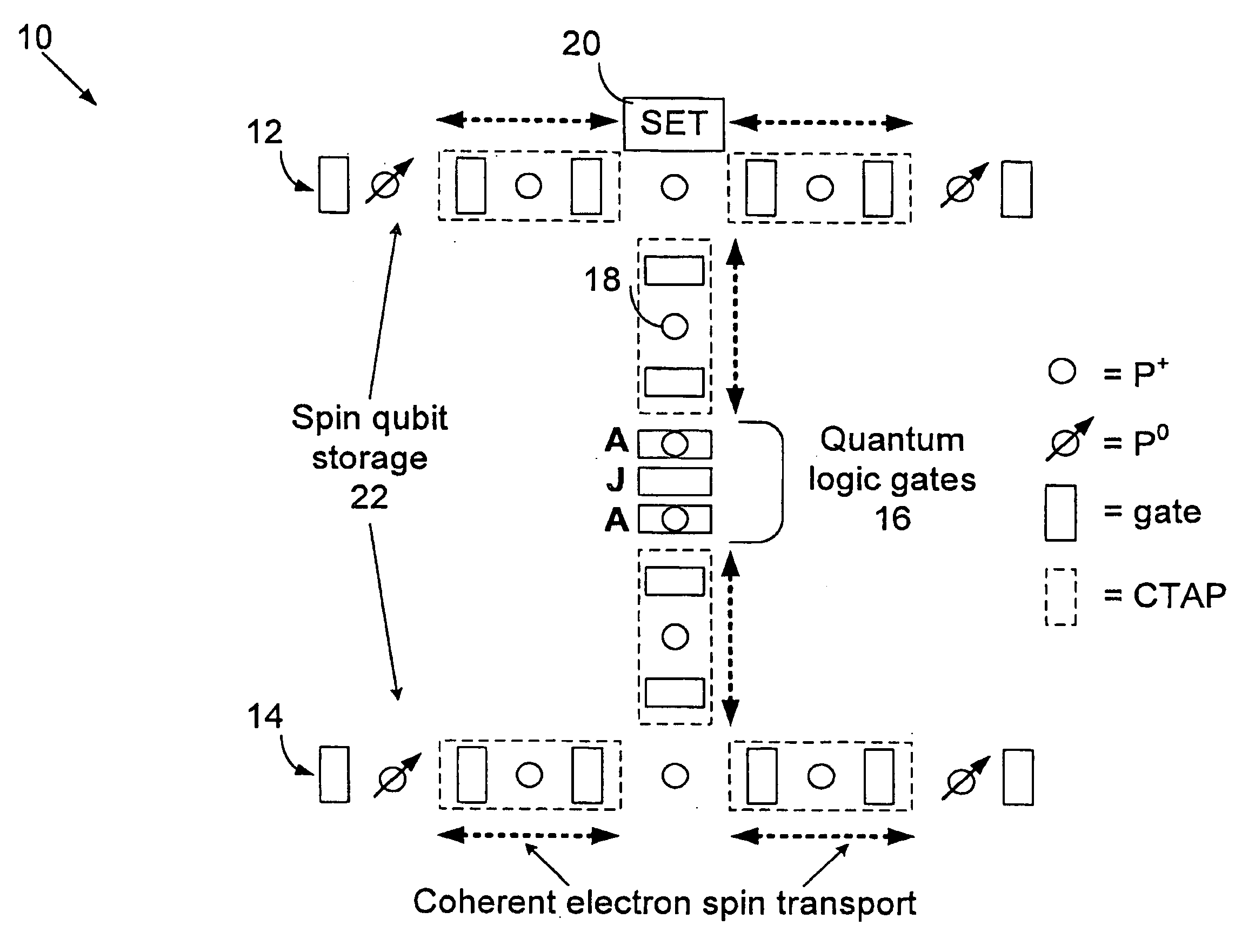
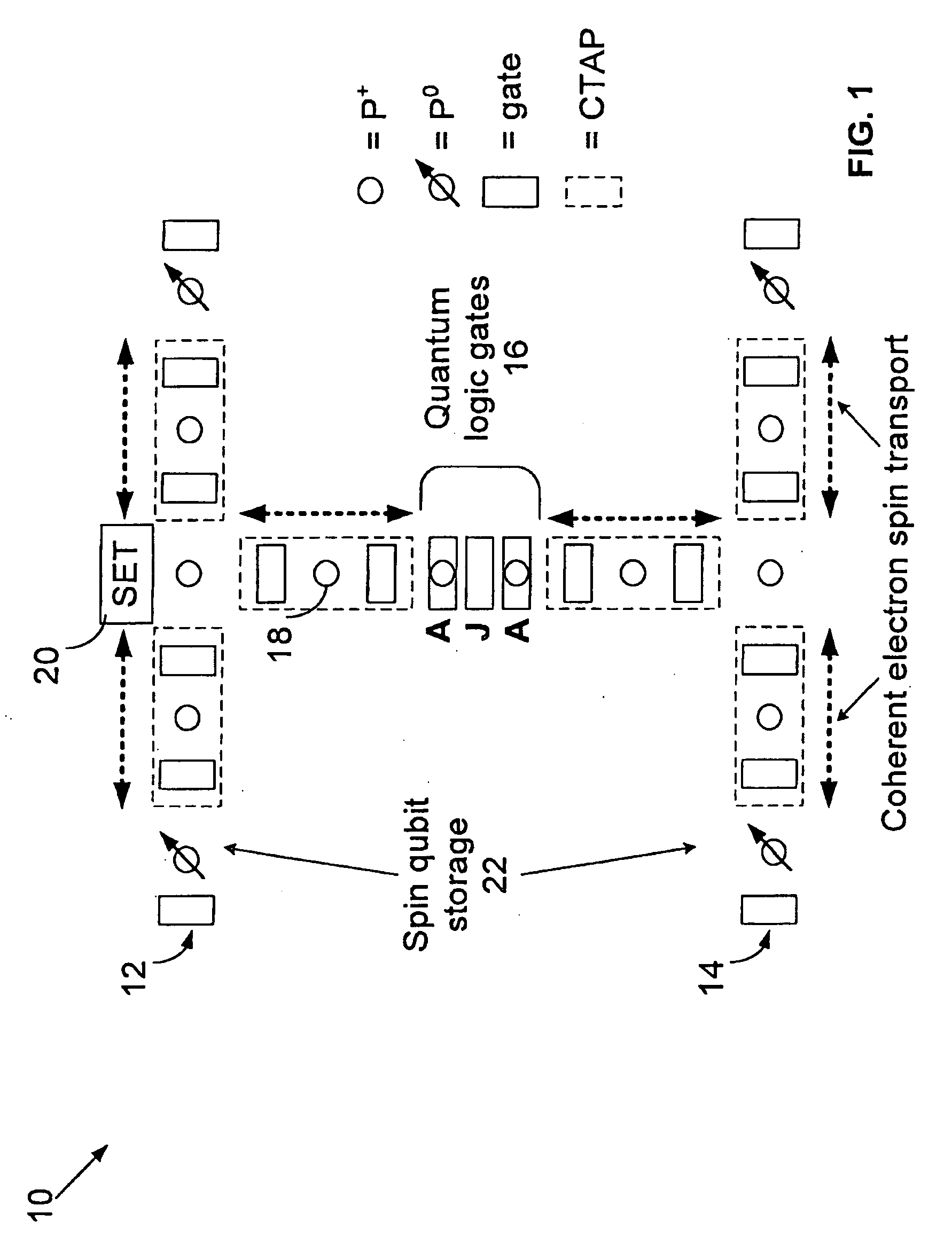
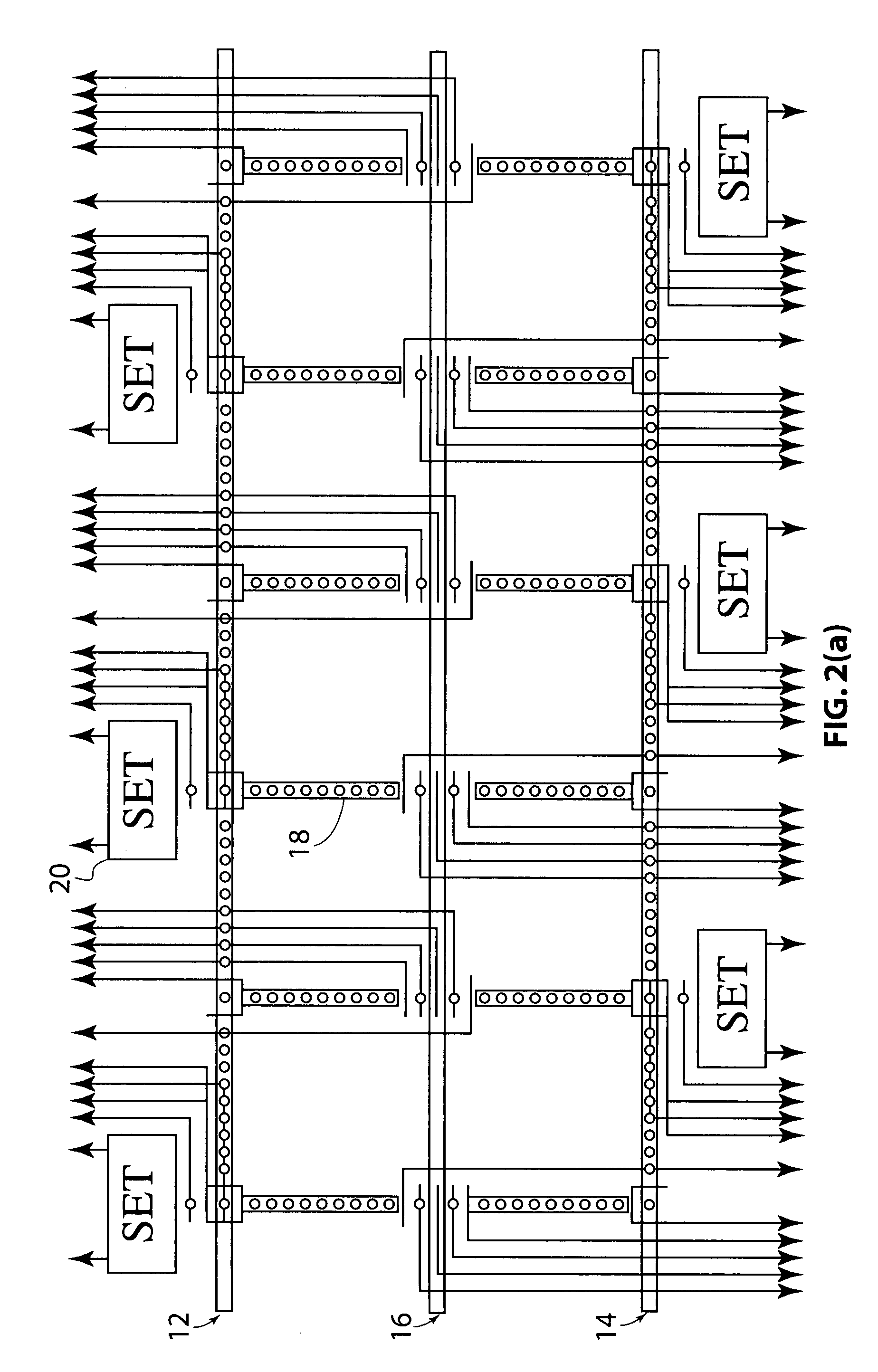
[0058]Referring first to FIG. 1, a quasi-two-dimensional donor architecture fundamental component structure 10 is described. In this example the computer architecture is related to a silicon based quantum computer in which the spin of electrons donated by phosphorus donor atom are used to form the qubits. An upper transport rail 12 and a lower transport rail 14 are arranged in parallel, and are interconnected by a quantum logic gate 16. Physical qubit sites, that is the phosphorus donor atoms, in the architecture are indicated by circles, one of which is identified at 18.

[0059]Periodically along the upper 12 and lower 14 transport rails there are sites for the initialisation or readout of qubits, or both, such as SET 20. There are also locations for qubit storage 22.

[0060]Transport around the architecture is achieved using a buried array of ionized donors D+ (which may be a spin zero species). These donors provide pathways for coherent transport of electron spins for in-place horizo...


PUM


Abstract

This invention concerns quantum error correction, that is the correction of errors in the transport and processing of qubits, by use of logical qubits made up of a plurality of physical qubits. The process takes place on a spatial array of physical qubit sites arranged with a quasi-2-dimensional topology having a first line of physical qubit sites and second line of physical qubit sites, where the first and second lines are arranged in parallel, with the sites of the first line in registration with corresponding sites in the second line. Between the first and second lines of physical qubit sites are a plurality of logic function gates, each comprised of a first physical qubit gate site associated with a first physical qubit site in the first line, and a second physical qubit gate site associated with the physical qubit site in the second line that corresponds to the first physical qubit site. The temporal process comprises the following steps: Creating a logical qubit in a section of the array by initialising an equal plurality of physical data and ancilla qubits at respective sites of the first and second lines within the section. Clocking each physical qubit site in the section at the same time. Permitting the physical data and ancilla qubits to move to an adjacent site in a clock cycle, provided that no site may contain more than one physical qubit at any time. Controlling the sites to achieve movement of ancilla qubits in the array to bring pairs of the ancilla qubits to respective first and second physical gate sites of logic function gates over the course of a number of clock cycles. Permitting logic operations to be performed at logic function gates which have both of their gate sites occupied by a physical ancilla qubit. Controlling the gate sites of the logic function gate to achieve the logic operation. Controlling the sites to achieve movement of the qubits in the array to bring pairs of all the data and ancilla qubits to respective logic function gates over the course of a number of clock cycles. Controlling the gate sites of the logic function gate to achieve the logic operation between each pair of data and ancilla qubits. Controlling the sites to achieve movement of the qubits in the array to bring all the data and ancilla qubits to respective sites where they can be read out. And, Using the values of the ancilla qubits read out to correct errors arising in the data qubits they have been gated with.

Description

TECHNICAL FIELD [0001]This invention concerns quantum error correction, that is the correction of errors in the transport and processing of qubits, by use of logical qubits made up of a plurality of physical qubits. In particular the invention concerns a method for error corrected computation, and in a further aspect an architecture with operational constraints.BACKGROUND ART [0002]The Kane paradigm of donor nuclear spin quantum computing in silicon [1] based on single atom placement fabrication techniques, [2,3] is an important realisation of Feynman's original concept of nanotechnology in the solid state. Variations on this theme include electron spin qubits [4-6] and charge qubits [7]. There are also possible realisations for quantum computers being investigated in Ion trap QCCD technologies [14], and GaAs 2e (S-T) qubits [15].[0003]Quantum computers are susceptible to error modes that do not trouble binary digital computers. For instance, gating errors and decoherence errors. Fa...

Claims


Application Information

Patent Timeline
Patent Type & Authority Applications(United States)
IPC IPC(8): H01L29/15
CPCG06N99/002B82Y10/00G06N10/00
Inventor HOLLENBERG, LLOYDSTEPHENS, ASHLEYGREENTREE, ANDREWFOWLER, AUSTINWELLARD, CAMERON
Owner NEWSOUTH INNOVATIONS PTY LTD
Why Eureka
Try Eureka