Magnetic field detector, and current detection device, position detection device and rotation detection devices using the magnetic field detector

a magnetic field and detector technology, applied in the direction of galvano-magnetic devices, instruments, record information storage, etc., can solve the problem of increasing power consumption and achieve the effect of stable output signal

Active Publication Date: 2008-08-07
MITSUBISHI ELECTRIC CORP
View PDF4 Cites 7 Cited by
  • Summary
  • Abstract
  • Description
  • Claims
  • Application Information

AI Technical Summary

Benefits of technology

[0017]In the magnetic field detector described above, the resistance change rate can be calibrated at any time without using the magnetic field generator. Also, by referring to a magnetoresistive element having the magnetic field response in the nonmagnetic field while an external magnetic field is applied thereto, output signals can be compared within the same detector, so that even in the case where the element sensitivity changes, a stable output signal can be produced.

Problems solved by technology

As a result, the power consumption is increased.

Method used


Image

  • Magnetic field detector, and current detection device, position detection device and rotation detection devices using the magnetic field detector
  • Magnetic field detector, and current detection device, position detection device and rotation detection devices using the magnetic field detector
  • Magnetic field detector, and current detection device, position detection device and rotation detection devices using the magnetic field detector

Examples


embodiment 1

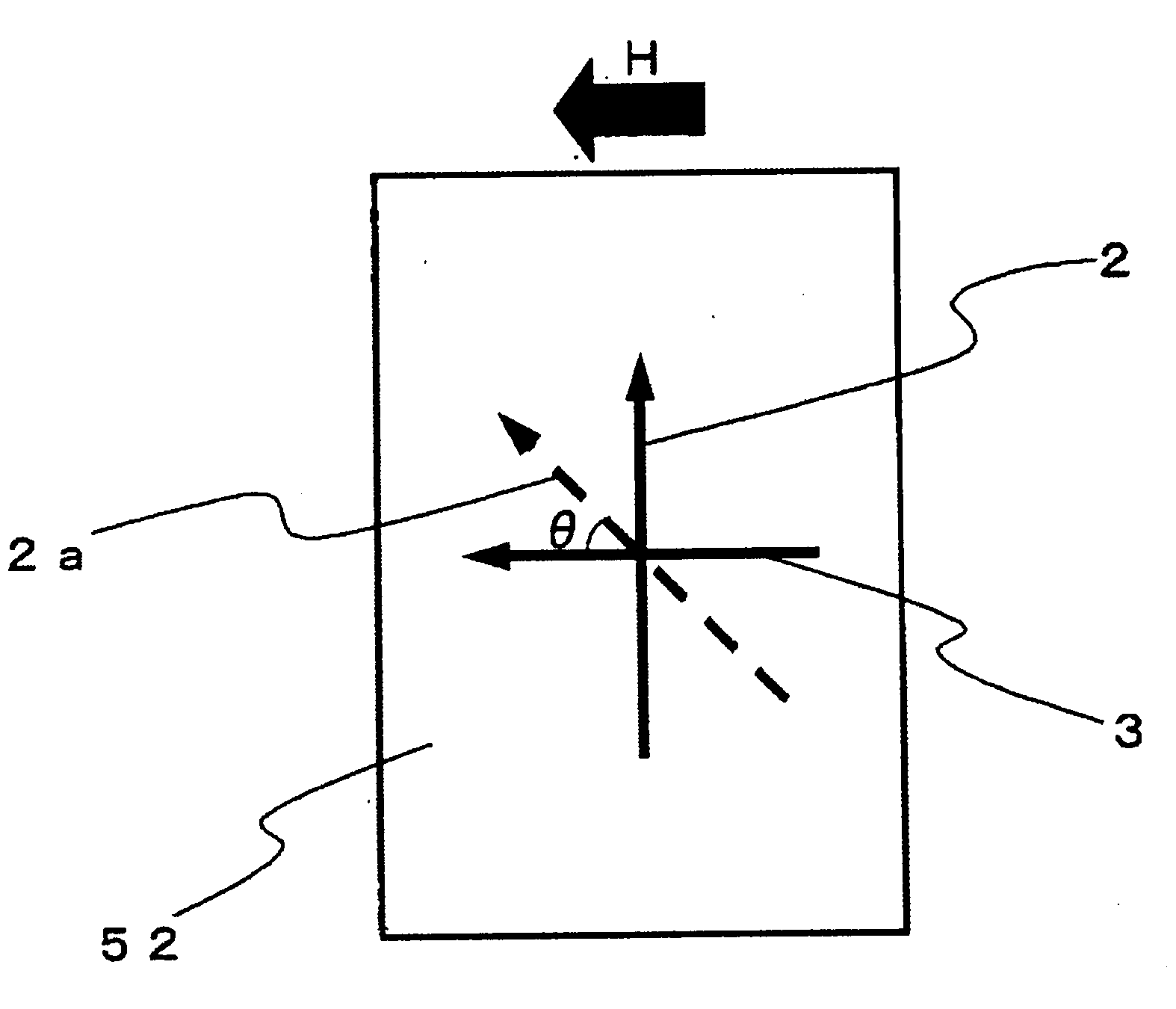
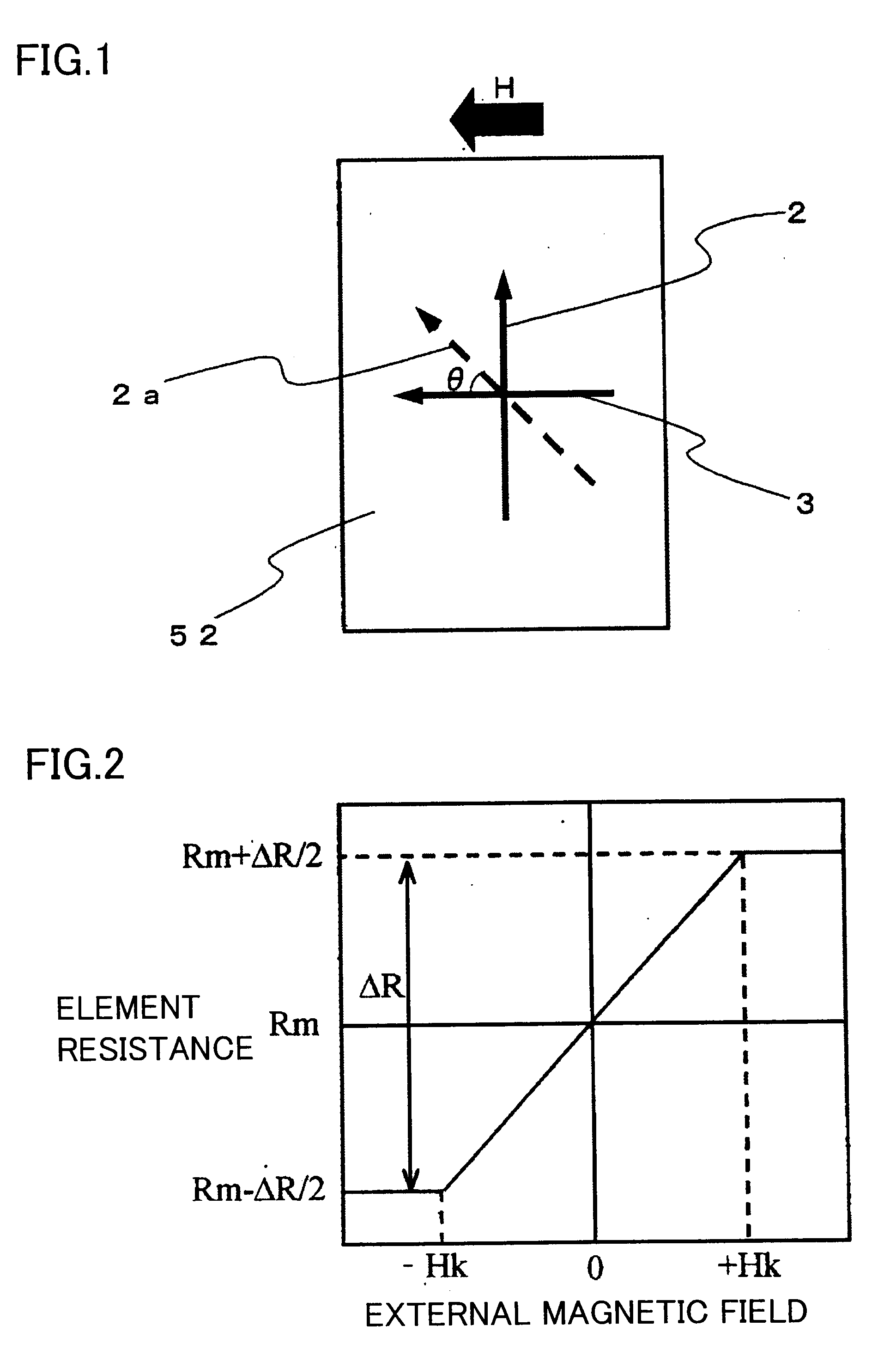
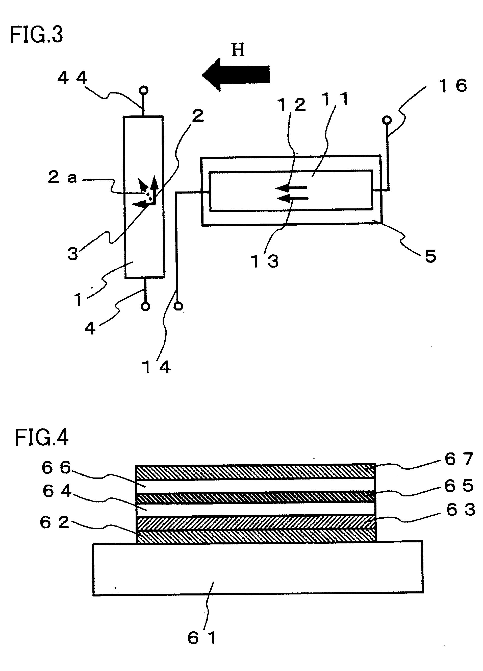
[0049]FIG. 3 is a plan view showing a magnetic field detector according to a first embodiment of the present invention. The shown magnetic field detector has one detecting magnetoresistive element 1 (hereinafter referred to as the detection element) and one reference magnetoresistive element 11 (hereinafter referred to as the reference element). The sectional structures of elements 1, 11 are shown in the schematic diagram of FIG. 4. In FIG. 4, a wiring layer 62 is formed on a substrate 61, and then an antiferromagnetic layer 63 is formed. Next, a first ferromagnetic layer 64 (fixed layer) of a ferromagnetic material with the direction of magnetization thereof fixed by antiferromagnetic layer 63 is formed. Further, a nonmagnetic layer 65 constituting an tunnel insulating layer is formed, above which a second ferromagnetic layer 66 (free layer) of a ferromagnetic material with the direction of magnetization changed by the external magnetic field is formed. Above second ferromagnetic l...

embodiment 2

[0078]According to this embodiment, as shown in FIG. 6, a bridge circuit is formed by adding a set of elements having the same configuration to detection element 1 and reference element 11 of the first embodiment. The detection element 41 and the reference element 51 added have the same configuration as detection element 1 and reference element 11, respectively, and therefore are not described again. Also, the directions of magnetization of the first and second ferromagnetic layers of detection elements 1 and 41 are the same. In this case, ΔV1 can be obtained by supplying the current from wires 7 to 77 and measuring the potential difference between wires 8 and 88.

[0079]According to this embodiment, the elements are formed as a bridge circuit and therefore a larger output can be obtained.

embodiment 3

[0080]FIG. 7 is a plan view showing a magnetic field detector according to a third embodiment of the present invention. The magnetic field detector according to this embodiment further includes a reference element 21 in the magnetic field detector according to the first embodiment. In this embodiment, the same component parts as those in the first embodiment are designated by the same reference numerals, respectively. Elements 1, 11, 21 have a similar stack structure to the first embodiment. In this embodiment, elements 1, 11, 21 are all formed in a rectangle. Elements 1, 11, 21 have not necessarily the same aspect ratio but have the same area to equalize the element resistance.

[0081]Of the directions of magnetization 3, 13, 23 of the first ferromagnetic layers of elements 1, 11, 21, direction of magnetization 3 and direction of magnetization 13 are parallel to each other, and direction of magnetization 13 and direction of magnetization 23 are antiparallel to each other. Direction o...


PUM

PropertyMeasurementUnit
angleaaaaaaaaaa
output voltageaaaaaaaaaa

Abstract

A magnetic field detector having a reference magnetoresistive element and a magnetic field detecting magnetoresistive element. The reference magnetoresistive element and the magnetic field detecting magnetoresistive element each has a stack structure including an antiferromagnetic layer, a fixed layer of a ferromagnetic material with the direction of magnetization fixed by the antiferromagnetic layer, a nonmagnetic layer, and a free layer of a ferromagnetic material with the direction of magnetization adapted to be changed by an external magnetic field. The reference magnetoresistive element is such that the direction of magnetization of the fixed layer and the direction of magnetization of the free layer in the nonmagnetic field are parallel or antiparallel to each other, and the magnetic field detecting magnetoresistive element is such that the direction of magnetization of the fixed layer and the direction of magnetization of the free layer in the nonmagnetic field are different from each other. Thus, it is possible to provide a magnetic field detector capable of singly calibrating the sensitivity and the resolution of the detector whenever required.

Description

CROSS REFERENCE TO RELATED APPLICATIONS AND INCORPORATION BY REFERENCE[0001]This application is a continuation of and claims the benefit of priority under 35 USC §120 from U.S. Ser. No. 10 / 589,246, filed Aug. 14, 2006, the entire content of which is incorporated herein by reference, which is the National Stage of PCT / JP04 / 13824, filed Sep. 22, 2004, and is based upon and claims the benefit of priority under 35 USC §119 from the Japanese Patent Applications No. 2004-043248, filed Feb. 19, 2004.TECHNICAL FIELD[0002]The present invention relates to a magnetic field detector for detecting the magnetic field by the giant magnetoresistance effect or the tunnel magnetoresistance effect, and a current detection device, a position detection device and a rotation detection device using the magnetic field detector.BACKGROUND ART[0003]The magnetoresistance (MR) effect is a phenomenon in which the electrical resistance is changed by application of a magnetic field to a ferromagnetic material, an...

Claims


Application Information

Patent Timeline
Patent Type & Authority Applications(United States)
IPC IPC(8): G11B5/33G01R33/09
CPCB82Y25/00G01R33/093G01R33/09G01R15/205
Inventor TAKENAGA, TAKASHIKOBAYASHI, HIROSHIKUROIWA, TAKEHARUBEYSEN, SADEHFURUKAWA, TAISUKE
Owner MITSUBISHI ELECTRIC CORP
Why Eureka
Try Eureka