Semiconductor device and memory and method of operating thereof

Active Publication Date: 2008-08-07
MACRONIX INT CO LTD
View PDF22 Cites 3 Cited by
  • Summary
  • Abstract
  • Description
  • Claims
  • Application Information

AI Technical Summary

Benefits of technology

[0007]The present invention is directed to providing a semiconductor device. On the same system, a metal oxide semiconductor transistor and a memory in th

Problems solved by technology

Therefore, the process of manufacturing the embedded memor

Method used


Image

  • Semiconductor device and memory and method of operating thereof
  • Semiconductor device and memory and method of operating thereof
  • Semiconductor device and memory and method of operating thereof

Examples


Example

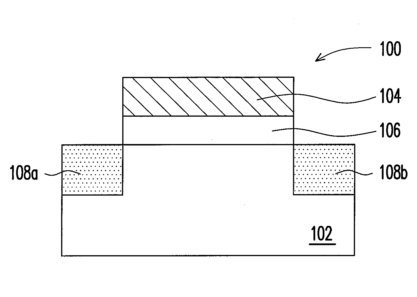
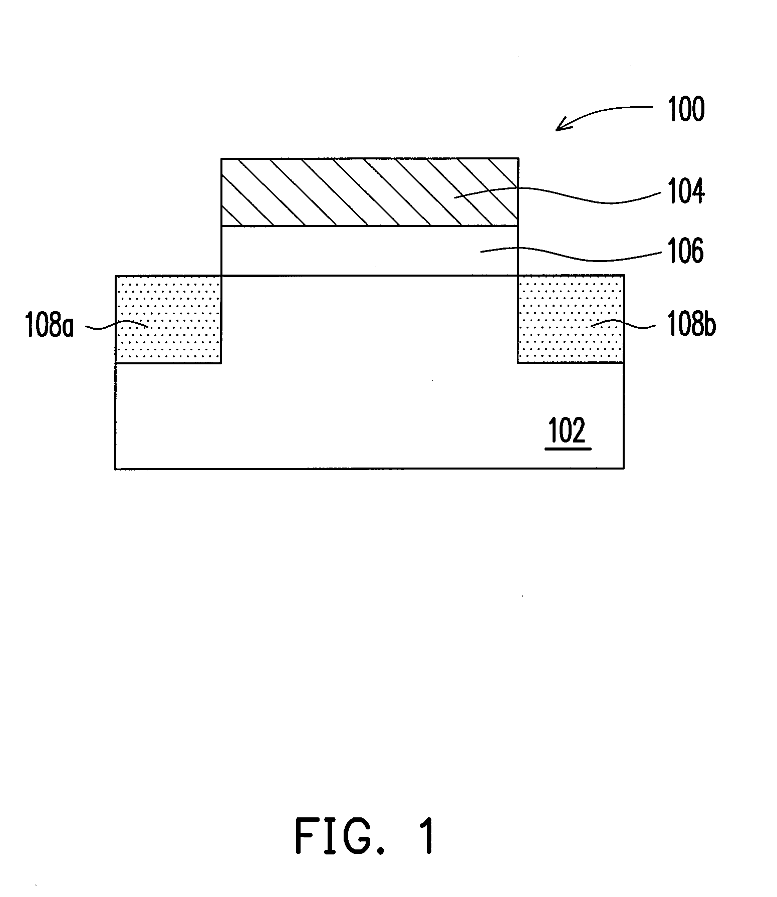
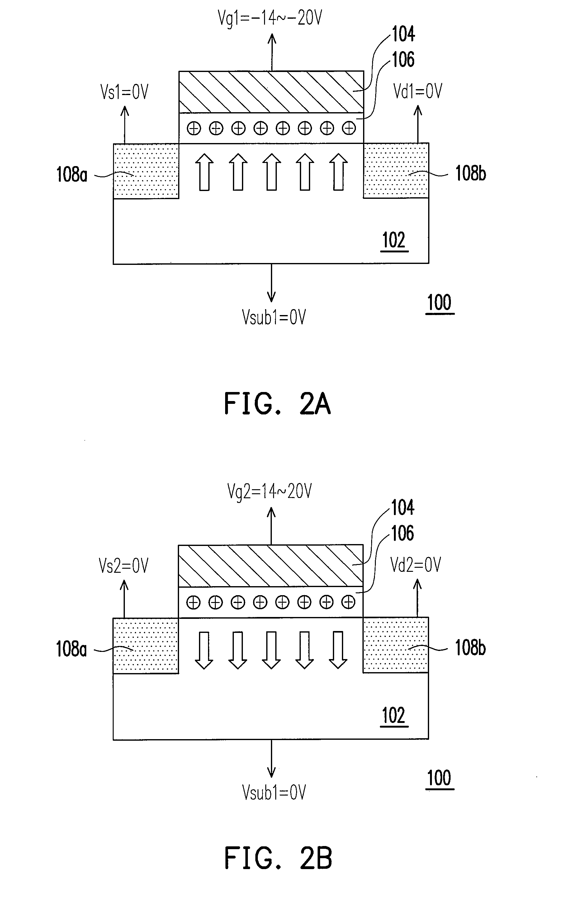
[0032]Reference will now be made in detail to the present preferred embodiments of the invention, examples of which are illustrated in the accompanying drawings. Wherever possible, the same reference numbers are used in the drawings and the description to refer to the same or like parts.

[0033]In integrated circuit of prior art, the elements of a memory and a logic circuit are integrated on the same system. And, the manufacturing process becomes difficult, thereby influencing the process yield. Therefore, a semiconductor device is provided to solve the above mentioned issues. The semiconductor device comprises a metal oxide semiconductor transistor disposed in the logic circuit region and a memory disposed in the memory region. The metal oxide semiconductor transistor comprising a substrate, a drain and a source disposed in the substrate, a gate disposed between the drain and the source and above the substrate, and a gate dielectric layer disposed between the gate and the substrate. ...


PUM


Abstract

A memory applicable to an embedded memory is provided. The memory includes a substrate, a gate, a charge-trapping gate dielectric layer, a source, and a drain. The gate is disposed above the substrate. The charge-trapping gate dielectric layer is disposed between the gate and the substrate. The source and the drain are disposed in the substrate beside the gate respectively.

Description

BACKGROUND OF THE INVENTION[0001]1. Field of the Invention[0002]The present invention relates to an integrated circuit. More particularly, the present invention relates to a semiconductor device and a memory having a structure similar to a transistor of a common logic device and a method of operating thereof.[0003]2. Description of Related Art[0004]Among various types of semiconductor devices, memories in which data can be stored, read out or erased and having the advantage that the data stored therein can be retained even after power is cut off has become a memory device widely applied in personal computers and electronic apparatuses.[0005]Generally speaking, in order to reduce the manufacturing cost of the semiconductor device and simplify the process, it gradually becomes a trend to integrate elements of a memory and a logic circuit on the same system, which is also known as an embedded memory. To be specific, in a conventional embedded memory structure, the transistor used as th...

Claims


Application Information

Patent Timeline
IPC IPC(8): G11C11/34H01L27/115
CPCG11C16/0466H01L27/11568H01L27/105H01L21/28282H01L29/40117H10B43/30
Inventor WU, CHAO-I
Owner MACRONIX INT CO LTD
Why Eureka
Try Eureka