
Semiconductor light emitting device

a technology of light-emitting devices and semiconductors, which is applied in the direction of semiconductor devices, basic electric elements, electrical equipment, etc., can solve the problems of reduced luminous efficiency, limited light extraction, and increased light loss, so as to maximize luminous efficiency, minimize reflection or absorption of emitted light, and uniform current spread

Active Publication Date: 2008-08-14
SAMSUNG ELECTRONICS CO LTD
View PDF13 Cites 66 Cited by
  • Summary
  • Abstract
  • Description
  • Claims
  • Application Information

AI Technical Summary

Benefits of technology

[0019]An aspect of the present invention provides a semiconductor light emitting device that minimizes reflection or absorption of emitted light, maximizes luminous efficiency with the maximum light emitting area, enables uniform current spreading with a small area electrode, and enables mass production with high reliability and high quality.

Problems solved by technology

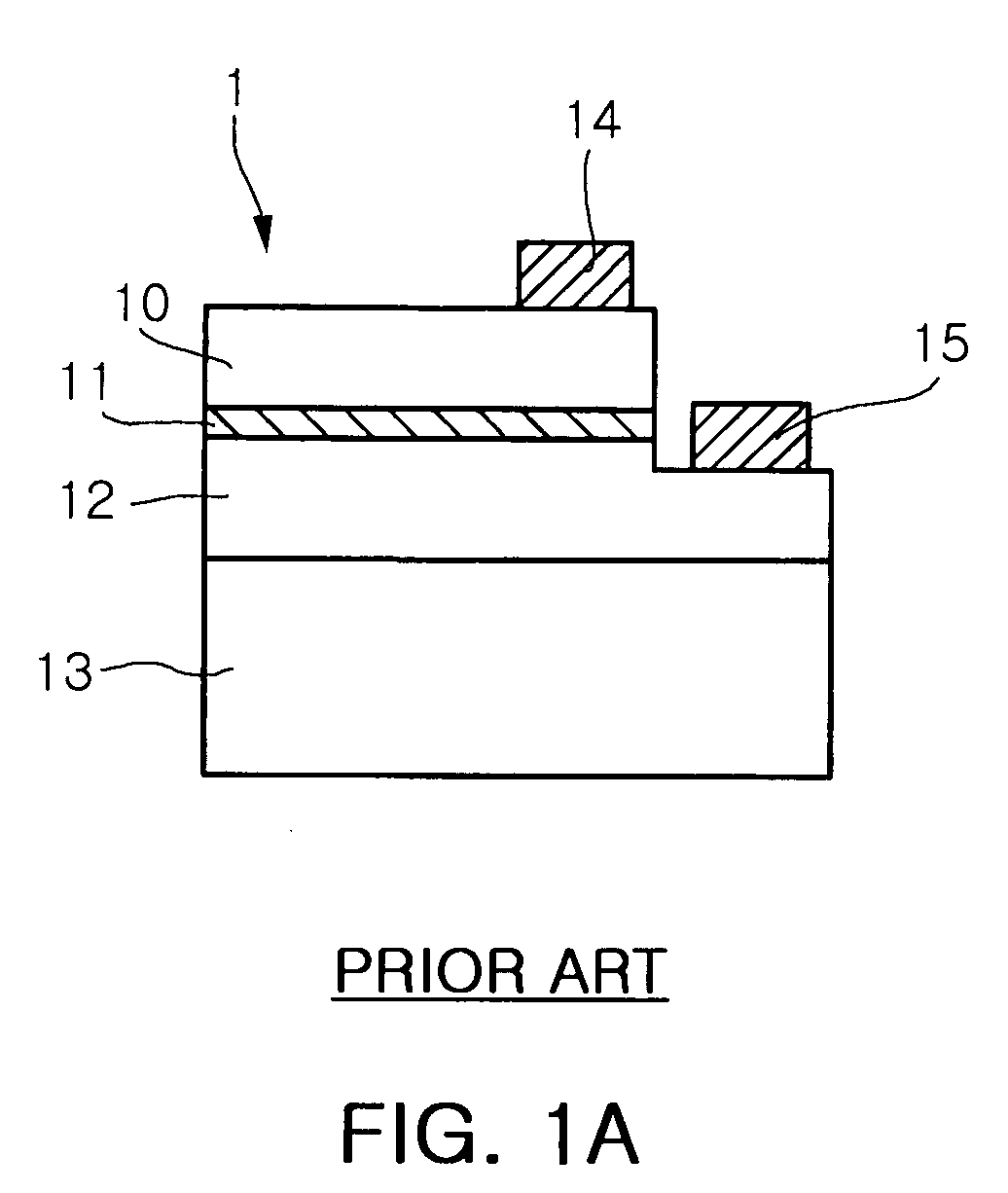
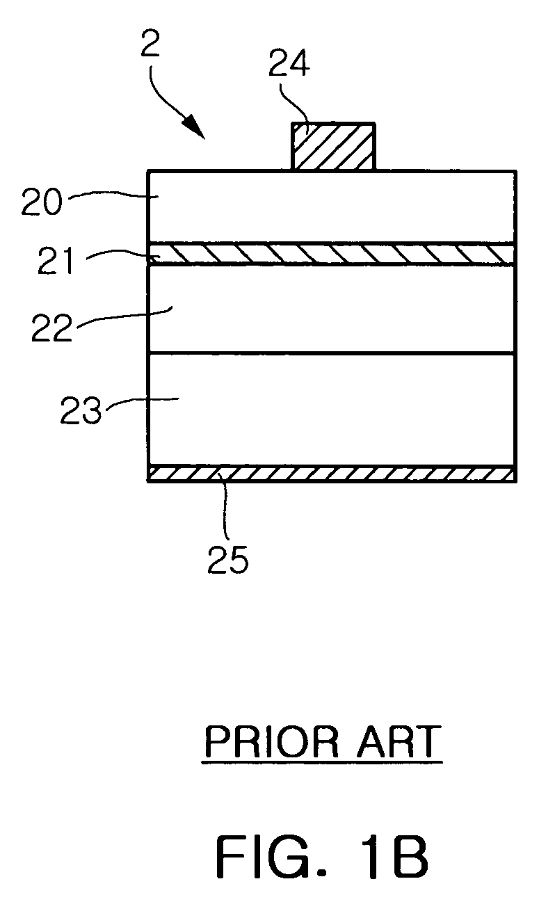
Therefore, light extraction is limited, light loss is caused by optical absorption, and luminous efficiency decreases.
For this reason, there is a need for expensive precision processing equipment.
This causes an increase in manufacturing costs, a decrease in productivity, a decrease in yield, and a decrease in product reliability.

Method used


Image

  • Semiconductor light emitting device
  • Semiconductor light emitting device
  • Semiconductor light emitting device

Examples


Embodiment Construction

[0040]Exemplary embodiments of the present invention will now be described in detail with reference to the accompanying drawings. This invention may, however, be embodied in many different forms and should not be construed as limited to the embodiments set forth herein. Rather, these embodiments are provided so that this disclosure will be thorough and complete, and will fully convey the scope of the invention to those skilled in the art.

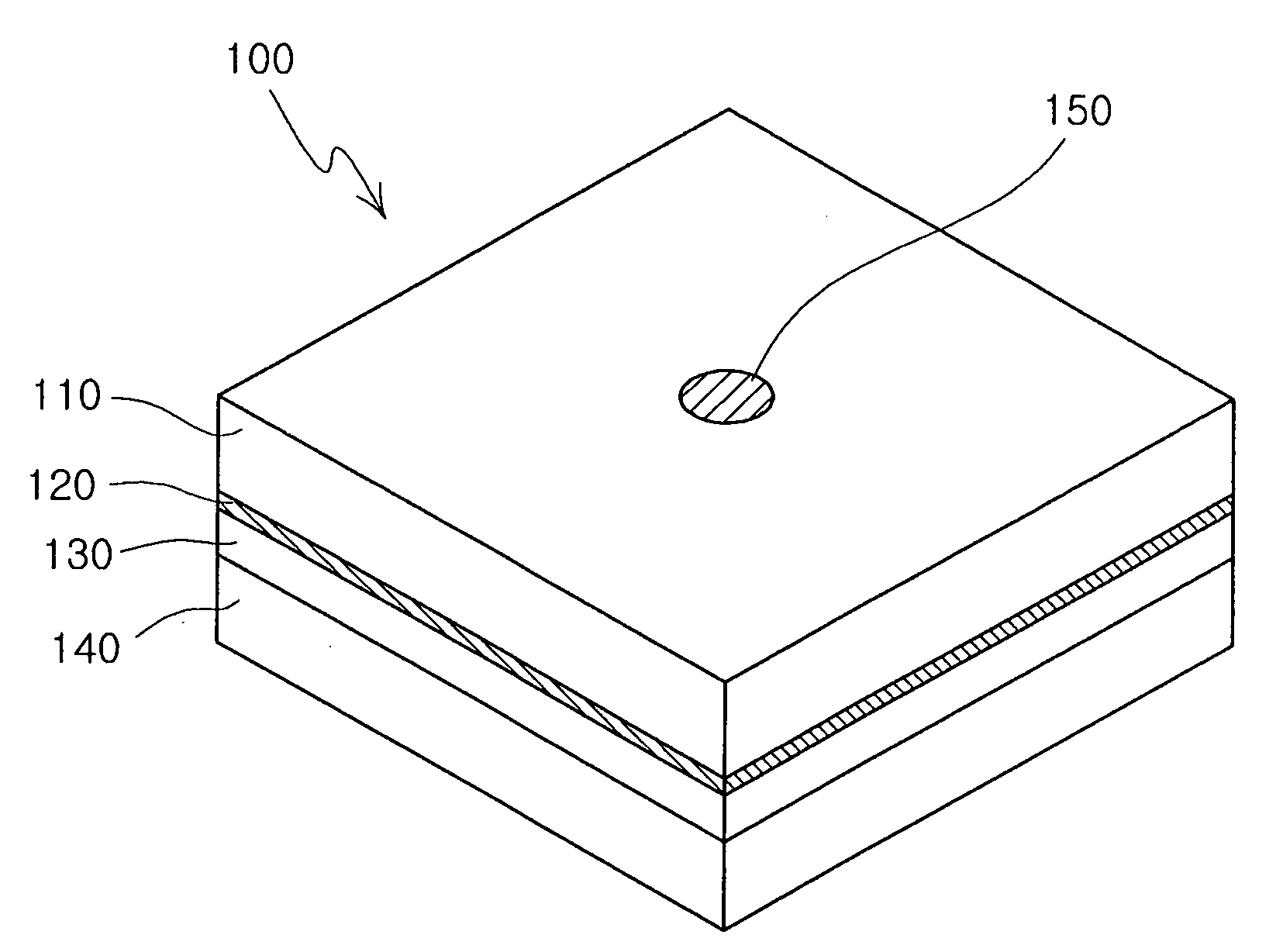
[0041]FIG. 2 is a cross-sectional view illustrating a semiconductor light emitting device according to one exemplary embodiment of the present invention. FIGS. 3A and 3B are top views illustrating the semiconductor light emitting device shown in FIG. 2. FIGS. 4A, 4B, and 4C are cross-sectional views illustrating the semiconductor light emitting device, shown in FIG. 3B, taken along the lines A-A′, B-B′, and C-C′, respectively.

[0042]A semiconductor light emitting device 100 according to the exemplary embodiment of the invention includes a conductive ...


PUM


Abstract

There is provided a semiconductor light emitting device that minimizes reflection or absorption of emitted light, maximizes luminous efficiency with the maximum light emitting area, enables uniform current spreading with a small area electrode, and enables mass production with high reliability and high quality. A semiconductor light emitting device according to an aspect of the invention includes first and second conductivity type semiconductor layers, an active layer formed therebetween, first electrode layer, and a second electrode part electrically connecting the semiconductor layers. The second electrode part includes an electrode pad unit, an electrode extending unit, and an electrode connecting unit connecting the electrode pad unit and electrode extending unit.

Description

CROSS-REFERENCE TO RELATED APPLICATIONS[0001]This application claims the priority of Korean Patent Application No. 2007-14844 filed on Feb. 13, 2007, in the Korean Intellectual Property Office, the disclosure of which is incorporated herein by reference.BACKGROUND OF THE INVENTION[0002]1. Field of the Invention[0003]The present invention relates to a semiconductor light emitting device, and more particularly, to a semiconductor light emitting device that minimizes reflection or absorption of emitted light, maximizes luminous efficiency with the maximum light emitting area, enables uniform current spreading with a small area electrode, and enables mass production with high reliability and high quality.[0004]2. Description of the Related Art[0005]Semiconductor light emitting devices include materials that emit light. For example, light emitting diodes (LEDs) are devices that use diodes, to which semiconductors are bonded, convert energy generated by combination of electrons and holes ...

Claims


Application Information

Patent Timeline
IPC IPC(8): H01L33/00H01L33/06H01L33/22H01L33/32H01L33/38H01L33/40
CPCH01L33/382H01L33/20
Inventor CHOI, PUN JAEPARK, KI YEOLLEE, SANG BUMMYOUNG, SEON YOUNGCHO, MYONG SOO
Owner SAMSUNG ELECTRONICS CO LTD
Learn More