Light Emitting Device With A Lens Of Silicone

a technology of light-emitting devices and silicone, applied in the direction of semiconductor devices, basic electric elements, electrical appliances, etc., can solve the problems of lens to encapsulant, reduced light extraction efficiency, and reduced light flux or yellowing

Inactive Publication Date: 2008-08-14
SEOUL SEMICONDUCTOR
View PDF14 Cites 55 Cited by
  • Summary
  • Abstract
  • Description
  • Claims
  • Application Information

AI Technical Summary

Benefits of technology

[0009]Another object of the present invention is to provide a light emitting device wherein the path of light emitted from a light emitting diode to be incident onto a lens can be simplified to easily design a lens.
[0010]To achieve the aforementioned objects of the present invention, the invention provides a light emitting device with a silicone lens. The light emitting device according to an embodiment of the invention comprises a heat sink. A package body surrounds at least a portion of the heat sink, and a light emitting diode is mounted on the heat sink. Meanwhile, the light emitting diode is covered with a silicone lens molded on the package body. The molded silicone lens can be employed to prevent reduction in light extraction efficiency due to poor bonding between a conventional lens and an encapsulant.
[0012]Meanwhile, a top surface of the light emitting diode is positioned at least above a top surface of the package body. In this case, since it is possible to prevent light emitted from the light emitting diode from being reflected on an inner wall of the package body, the path of light incident on the silicone lens can be easily predicted, and thus, the design of lens can also be easily made. The position of the top surface of the light emitting diode is set in accordance with the height of the top surface of the heat sink. The top surface of the heat sink is positioned near the top surface of the package body so that the top surface of the light emitting diode can be positioned at least above the top surface of the package body. The top surface of the heat sink can be positioned in the same plane as or higher than that of the package body.
[0013]A silicone encapsulant may be interposed between the silicone lens and the light emitting diode to cover the light emitting diode. Each of the encapsulant and the lens is made of a silicone material. Since the silicone lens is particularly molded on the encapsulant, the reduction in light extraction efficiency due to refractive index difference and poor bonding between lens and encapsulant can be prevented. Meanwhile, the silicone lens and / or silicone encapsulant may contain a phosphor capable of converting the wavelength of light emitted from the light emitting diode. Accordingly, a light emitting diode that generates a single wavelength can be employed to implement multicolored light, e.g. white light.
[0015]According to the embodiment of the present invention, a light emitting device can be provided wherein a silicone lens molded on a package body is employed to prevent the reduction in light extraction efficiency due to poor interface between encapsulant and lens. Further, a light emitting device can be provided wherein the path of light emitted from a light emitting diode to be incident on a lens can be simplified to easily design the lens.

Problems solved by technology

However, since the epoxy resin causes the disconnection of the bonding wire due to its relatively large hardness and absorbs short wavelength visible light, there are problems of reduction in light flux or yellowing.
However, a prior art for attaching a lens to an encapsulant may lower light extraction efficiency due to poor bonding or refractive index difference between encapsulant and lens, or the like.
Further, in a case where a light emitting diode is mounted within a recess of a package body, it is difficult to predict the path of light emitted to the outside due to light reflection produced on a sidewall of the recess or on an interface between an encapsulant and a lens.
Since it is difficult to predict the path of light emitted from a light emitting diode to be incident onto a lens, it is difficult to design a lens capable of precisely adjusting a required viewing angle or emission direction of light.

Method used


Image

  • Light Emitting Device With A Lens Of Silicone
  • Light Emitting Device With A Lens Of Silicone
  • Light Emitting Device With A Lens Of Silicone

Examples


Embodiment Construction

[0019]Hereinafter, a preferred embodiment of the present invention will be described in detail with reference to the accompanying drawings. The following embodiment is provided only as an example to fully convey the spirit and scope of the present invention to those skilled in the art. Therefore, the present invention is not limited to the following embodiment but may be implemented in various other forms. In the drawings, the width, length, thickness and the like of components may be exaggerated for convenience of illustration. Like reference numerals indicate like elements throughout the specification and drawings.

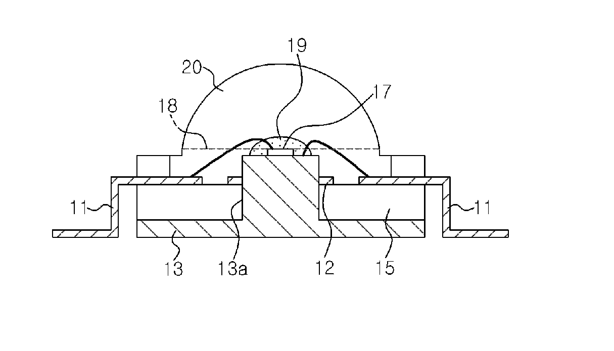
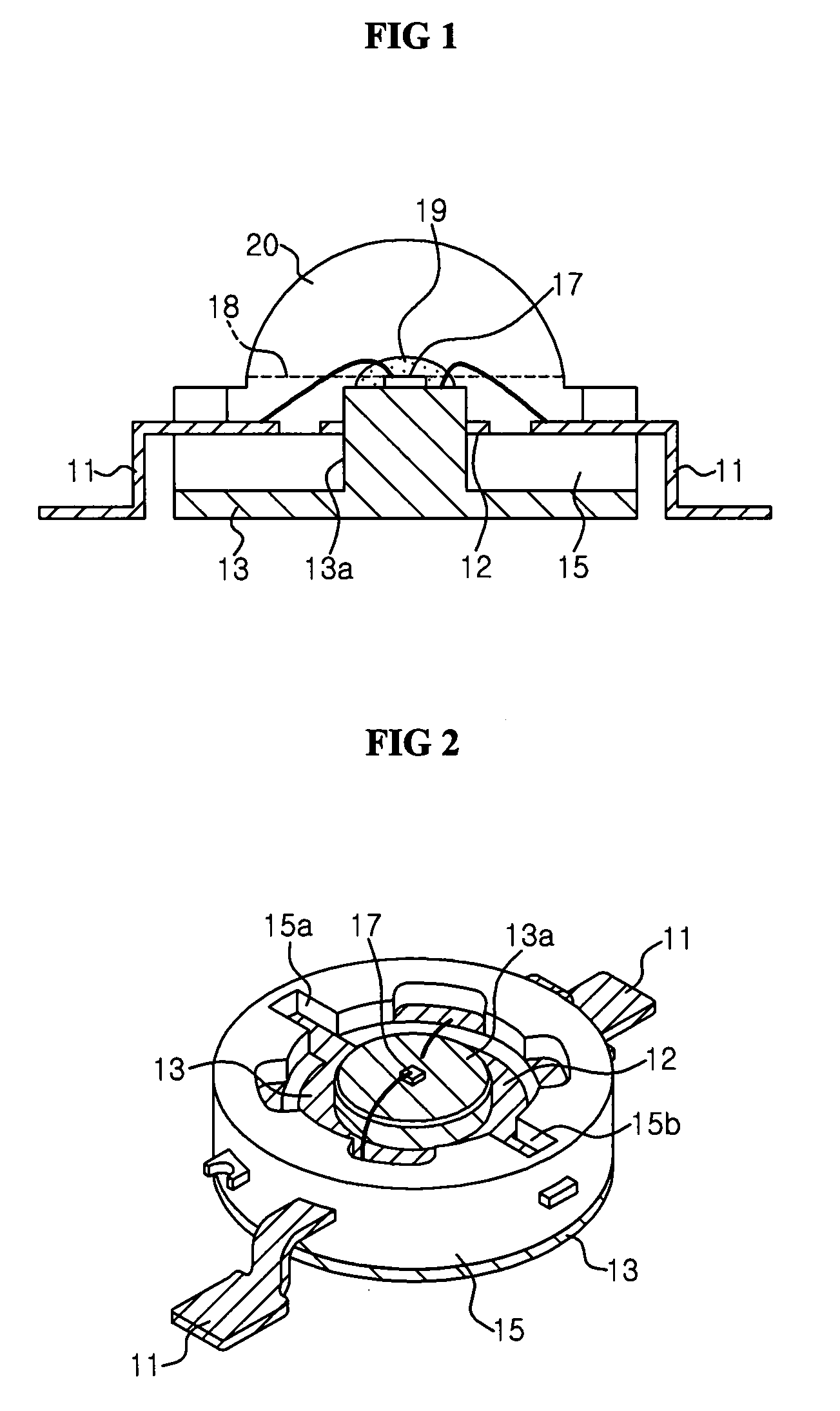
[0020]FIGS. 1 and 2 are sectional and perspective views illustrating a light emitting device according to an embodiment of the present invention.

[0021]Referring to FIGS. 1 and 2, a package body 15 surrounds a heat sink 13. The heat sink 13 is fitted into a support ring 12 such that it is possible to prevent the heat sink from being separated from the package body 15.

[002...


PUM


Abstract

Disclosed herein is a light emitting device with a silicone lens. The light emitting device comprises a heat sink. A package body surrounds at least a portion of the heat sink, and a light emitting diode is mounted on the heat sink. Meanwhile, the light emitting diode is covered with a silicone lens molded on the package body. The molded silicone lens can be employed to prevent reduction in light extraction efficiency due to poor bonding between lens and encapsulant.

Description

RELATED APPLICATION[0001]This application is a U.S. national phase application of PCT International Application No. PCT / KR2006 / 002943, filed Jul. 26, 2006, which claims priority of Korean Patent Application No. 2005-070271, filed Aug. 1, 2005, the contents of which are incorporated herein by reference in their entirety.FIELD OF THE INVENTION[0002]The present invention relates to a light emitting device, and more particularly, to a light emitting device with a silicone lens formed by molding a silicone encapsulant into a lens shape to improve light extraction efficiency and simplify a manufacturing process.BACKGROUND OF THE INVENTION[0003]In general, a light emitting device comprises a package body with a recess and a light emitting diode mounted within the recess of the package body. The light emitting diode has advantages in that it has a smaller size, a longer life span and lower power consumption as compared with an incandescent bulb, a fluorescent lamp and a discharge light sour...

Claims


Application Information

Patent Timeline
Patent Type & Authority Applications(United States)
IPC IPC(8): H01L33/00H01L33/54H01L33/58H01L33/64
CPCH01L33/54H01L33/642H01L33/58H01L2224/48091H01L2224/48247H01L2224/8592H01L2924/181H01L2924/19107H01L2924/00014H01L2924/00012
Inventor LEE, CHUNG HOONKIM, DO HYUNG
Owner SEOUL SEMICONDUCTOR
Why Eureka
Try Eureka