Semiconductor device

Inactive Publication Date: 2008-08-14
SEMICON ENERGY LAB CO LTD
View PDF6 Cites 33 Cited by
  • Summary
  • Abstract
  • Description
  • Claims
  • Application Information

AI Technical Summary

Benefits of technology

[0014]According to the invention, in the semiconductor device, the size of the integrated circuit portion can be close to the desired size of the antenna, and the integrated circuit portion and the antenna are easily connected. Thus, the semiconductor device can surely transmit and receive a sig

Problems solved by technology

However, connection of a connection terminal of the minute integrated circuit portion and connection terminals at one end and the other end of the antenna in the semiconductor device causes reduction in yield due to bad conne

Method used


Image

  • Semiconductor device
  • Semiconductor device
  • Semiconductor device

Examples


embodiment mode 1

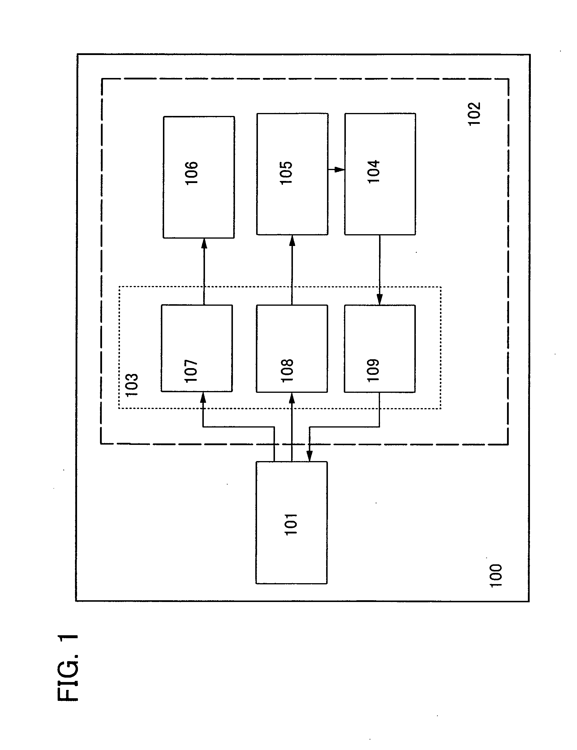
[0042]A structure of a semiconductor device of the invention is described with reference to FIG. 1.

[0043]FIG. 1 shows a structure example of a block diagram of a semiconductor device used in the invention. The semiconductor device shown in FIG. 1 includes an antenna 101 and an integrated circuit portion 102 over a substrate 100. The integrated circuit portion 102 is provided with a transmission / reception circuit 103, a memory circuit 104, a memory control circuit 105, and a power supply circuit 106. The transmission / reception circuit 103 includes a rectification circuit 107, a demodulation circuit 108, and a modulation circuit 109.

[0044]The transmission / reception circuit 103 shown in FIG. 1 has a rectification function in which electric power of an electromagnetic wave received by the antenna 101 (hereinafter referred to as a wireless signal) is converted into a power supply potential, a demodulation function in which data is extracted from the wireless signal, and a modulation func...

embodiment mode 2

[0079]In this embodiment mode, a structure which is different from those of the semiconductor device of the invention described in Embodiment Mode 1 is described.

[0080]FIG. 8 shows a structure example of a block diagram of a semiconductor device described in this embodiment mode. The semiconductor device shown in FIG. 8 includes an antenna 801, an integrated circuit portion 802, and a booster antenna 811 over a substrate 800. The integrated circuit portion 802 is provided with a transmission / reception circuit 803, a memory circuit 804, a memory control circuit 805, and a power supply circuit 806. The transmission / reception circuit 803 includes a rectification circuit 807, a demodulation circuit 808, and a modulation circuit 809.

[0081]This embodiment mode is different from the structure of FIG. 1 in Embodiment Mode 1 in that the booster antenna is included. In FIG. 8, the booster antenna 811 is included. The booster antenna described in this embodiment mode refers to an antenna which...

embodiment mode 3

[0113]This embodiment mode describes a structure and an operation of a semiconductor device of the invention in the case where a battery is provided.

[0114]A structure of a semiconductor device of the invention in the case where a battery is provided is described with reference to FIG. 15. FIG. 15 shows a structure example of a block diagram of a semiconductor device described in this embodiment mode. The semiconductor device shown in FIG. 15 includes an antenna 1501, an integrated circuit portion 1502, and a battery 1550 over a substrate 1500. The integrated circuit portion 1502 is provided with a transmission / reception circuit 1503, a memory circuit 1504, a memory control circuit 1505, and a power supply circuit 1506. The transmission / reception circuit 1503 includes a rectification circuit, a demodulation circuit, and a modulation circuit.

[0115]This embodiment mode is different from Embodiment Modes 1 and 2 in that a battery is provided. The semiconductor device described in this e...


PUM


Abstract

A semiconductor device, in which an integrated circuit portion and an antenna are easily connected, can surely transmit and receive a signal to and from a communication device. The integrated circuit portion is formed of a thin film transistor over a surface of a substrate so that the area occupied by the integrated circuit portion is increased. The antenna is provided over the integrated circuit portion, and the thin film transistor and the antenna are connected. Further, the area over the substrate occupied by the integrated circuit portion is 0.5 to 1 times as large as the area of the surface of the substrate. Thus, the size of the integrated circuit portion can be close to the desired size of the antenna, so that the integrated circuit portion and the antenna are easily connected and the semiconductor device can surely transmit and receive a signal to and from the communication device.

Description

BACKGROUND OF THE INVENTION[0001]1. Field of the Invention[0002]The present invention relates to a semiconductor device. In particular, the present invention relates to a semiconductor device which performs wireless communication using an electromagnetic wave.[0003]2. Description of the Related Art[0004]In recent years, an individual identification technology which utilizes an electromagnetic wave for wireless communication has attracted attention. In particular, an individual identification technology that utilizes a semiconductor device using an RFID (Radio Frequency Identification), which is also referred to as an IC (Integrated Circuit) chip, an RF tag, a wireless tag, or an electronic tag, as a semiconductor device that communicates data by wireless communication has attracted attention. The individual identification technology that utilizes a semiconductor device using an RFID (hereinafter also referred to as a semiconductor device) has started to help production, management, ...

Claims


Application Information

Patent Timeline
IPC IPC(8): H01L23/02
CPCH01L23/5227H01L27/0203H01L27/12H01L27/1214H01L27/1266H01L27/13H01L27/0688H01L2924/0002H01L2924/3011H01L23/528G06K19/07722G06K19/07775H01L2924/00H01L27/1277H01L27/1225
Inventor KOYAMA, JUNYAMAZAKI, SHUNPEI
Owner SEMICON ENERGY LAB CO LTD
Why Eureka
Try Eureka