

Interconnect structure with bi-layer metal cap
- Summary
- Abstract
- Description
- Claims
- Application Information
AI Technical Summary
Problems solved by technology
Method used
Image

Examples
second embodiment
[0037]With reference to FIGS. 9-13, an interconnect structure with bi-layer metal cap is described. In this particular embodiment, the interconnect features are formed within a dielectric layer and a hardmask layer, as described in detail hereinbelow.
first embodiment
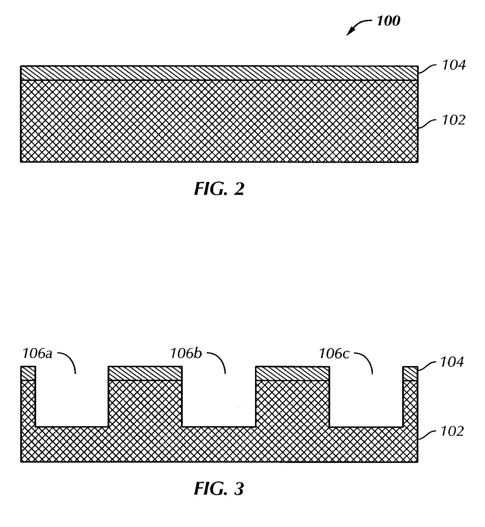
[0038]With initial reference to FIG. 9, a semiconductor structure 200 includes a first dielectric layer 202, a hardmask 204 formed on dielectric layer 202 and interconnect feature 208 formed on a plurality of lines 206a, 260b and 206c. It is noted that, hardmask 204 is not removed from dielectric layer 202 after the planarization process, as described hereinabove with respect to the Interconnect features 208 include a conductive material layer 210 and a barrier or liner 212 formed about lines 206a, 206b and 206c, to prevent conductive material 210 from diffusing.
[0039]With reference to FIG. 10, a blanket deposition of a first metal cap 214 is formed over the patterned structure using suitable deposition techniques. Metal residue 216 is observed on a top surface of dielectric layer 202.
[0040]With reference to FIG. 11, a NH3 / N2 plasma ash / surface treatment 218 is performed over the structure for creating a metal nitride 220 on a top surface of metal cap 214, and a damaged dielectric ...
PUM
 Abstract
Description
Claims
Application Information