Self-aligned contacts for nanowire field effect transistors

a field effect transistor and self-aligning technology, applied in the field of self-aligning contacts of nanowire field effect transistors, can solve the problems of undesirable junction doping profile or unsatisfactory amorphization of nanowires

Active Publication Date: 2011-06-09
GLOBALFOUNDRIES US INC
View PDF68 Cites 58 Cited by
  • Summary
  • Abstract
  • Description
  • Claims
  • Application Information

AI Technical Summary

Benefits of technology

[0004]In one aspect of the present invention, a method for forming a nanowire field effect transistor (FET) device includes forming a nanowire over a semiconductor substrate, forming a gate structure around a portion of the nanowire, forming a capping layer on the gate structure; forming a first spacer adjacent to sidewalls of the gate and around portions of nanowire extending from the gate, forming a hardmask layer on the capping layer and the first spacer, removing exposed portions of the nanowire, epitaxially growing a doped semiconductor material on exposed cross sections of the nanowire to form a source region and a drain region, forming a silicide material in the epitaxially grown doped semiconductor material, forming a conductive material on the source and drain regions, and forming an isolation region around the device.
[0005]In another aspect of the present invention, a method for forming a nanowire field effect transistor (FET) device includes forming a nanowire over a semiconductor substrate, forming a gate structure around a portion of the nanowire, forming a capping layer on the gate structure, forming a first spacer adjacent to sidewalls of the gate and around portions of nanowire extending from the gate, forming a hardmask layer on the capping layer and the first spacer, removing exposed portions of the nanowire, doping the exposed portions of the nanowire to form source and drain regions, forming a silicide material in the source and drain regions of the exposed portions of the nanowire, forming a conductive material on the source and drain regions, and forming an isolation region around the device.
[0006]In yet another aspect of the present invention, a nanowire field effect transistor (FET) device includes a channel region including a silicon portion having a first distal end extending from the channel region and a second distal end extending from the channel region, the silicon portion is partially surrounded by a gate structure disposed circumferentially around the silicon portion, a polysilicon capping layer having a silicide portion disposed on the gate structure, a source region having a silicide portion, the source region including a first doped epi-silicon nanowire extension contacting the first distal end of the silicon portion, a drain region having a silicide portion, the drain region including a second doped epi-silicon nanowire extension contacting the second distal end of the silicon portion, a first conductive member contacting the silicide portion of the polysilicon capping layer, a second conductive member contacting the silicide portion of the source region, and a third conductive member contacting the silicide portion of the drain region.

Problems solved by technology

Previous fabrication methods that used ion-implantation to dope the small diameter nanowire may result in undesirable amorphization of the nanowire or an undesirable junction doping profile.

Method used


Image

  • Self-aligned contacts for nanowire field effect transistors
  • Self-aligned contacts for nanowire field effect transistors
  • Self-aligned contacts for nanowire field effect transistors

Examples


Embodiment Construction

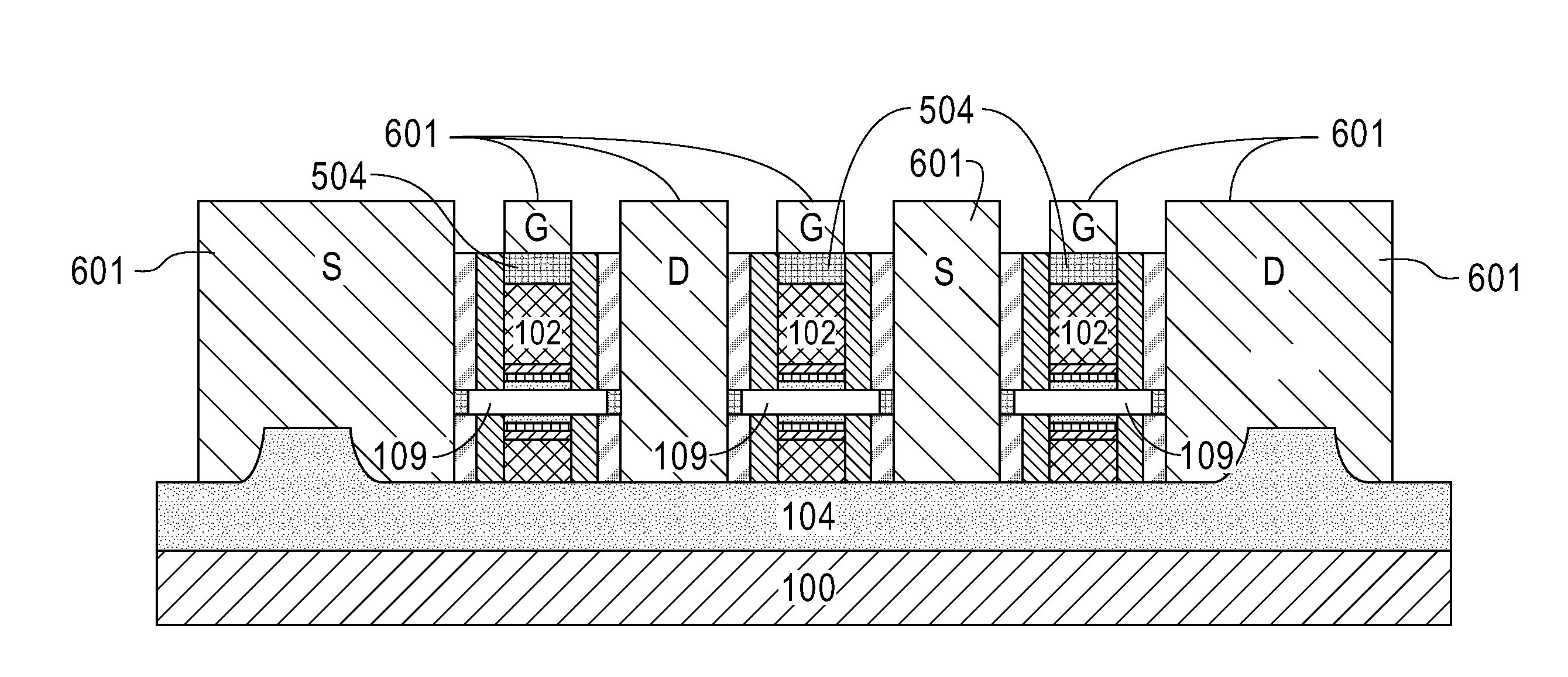
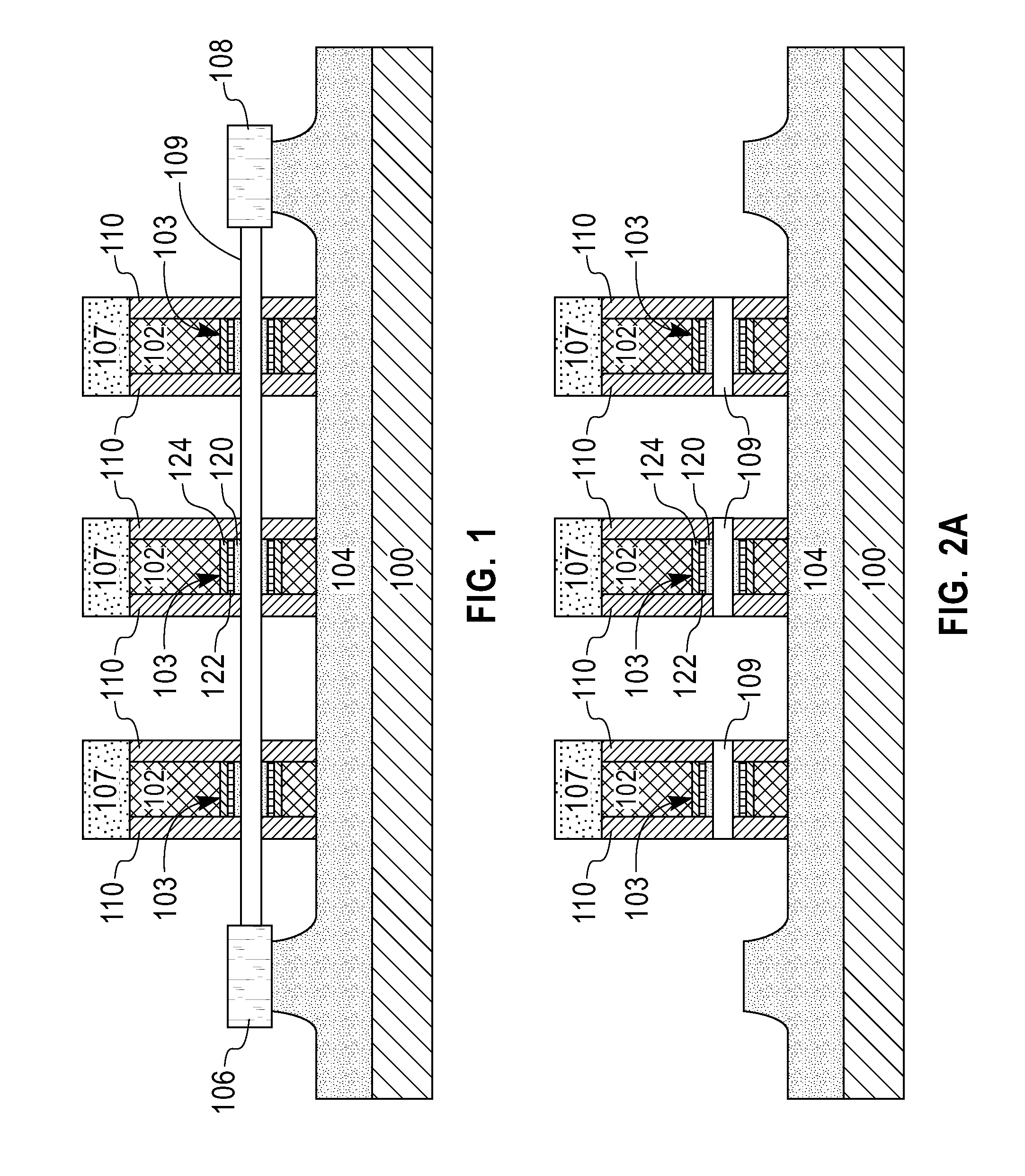
[0011]FIG. 1 illustrates a cross-sectional view of a plurality of FET devices. A silicon on insulator (SOI) pad region 106, pad region 108, and nanowire portion 109 are defined on a buried oxide (BOX) layer 104 that is disposed on a silicon substrate 100. The pad region 106, pad region 108, and nanowire portion 109 may be patterned by the use of lithography followed by an etching process such as, for example, reactive ion etching (RIE). Once the pad region 106, pad region 108, and nanowire portion 109 are patterned, an isotropic etching process suspends the nanowires 109 above the BOX layer 104. Following the isotropic etching, the nanowire portions 109 may be smoothed to form elliptical shaped (and in some cases, cylindrical shaped) nanowires 109 that are suspended above the BOX layer 104 by the pad region 106 and the pad region 108. An oxidation process may be performed to reduce the diameter of the nanowires 109 to desired dimensions.

[0012]Once the nanowires 109 are formed, gates...


PUM


Abstract

A method for forming a nanowire field effect transistor (FET) device includes forming a nanowire over a semiconductor substrate, forming a gate structure around a portion of the nanowire, forming a capping layer on the gate structure; forming a first spacer adjacent to sidewalls of the gate and around portions of nanowire extending from the gate, forming a hardmask layer on the capping layer and the first spacer, removing exposed portions of the nanowire, epitaxially growing a doped semiconductor material on exposed cross sections of the nanowire to form a source region and a drain region, forming a silicide material in the epitaxially grown doped semiconductor material, and forming a conductive material on the source and drain regions.

Description

CROSS REFERENCE TO RELATED APPLICATIONS[0001]This application is related to co-pending application docket numbers YOR920090398US1, YOR920090399US1, YOR920090411US1, YOR920090414US1, YOR920090506US1, all of which are incorporated by reference herein.FIELD OF INVENTION[0002]The present invention relates to semiconductor nanowire field effect transistors.DESCRIPTION OF RELATED ART[0003]A nanowire field effect transistor (FET) includes doped portions of nanowire that contact the channel region and serve as source and drain regions of the device. Previous fabrication methods that used ion-implantation to dope the small diameter nanowire may result in undesirable amorphization of the nanowire or an undesirable junction doping profile.BRIEF SUMMARY[0004]In one aspect of the present invention, a method for forming a nanowire field effect transistor (FET) device includes forming a nanowire over a semiconductor substrate, forming a gate structure around a portion of the nanowire, forming a ca...

Claims


Application Information

Patent Timeline
Patent Type & Authority Applications(United States)
IPC IPC(8): H01L29/66H01L21/336
CPCB82Y10/00B82Y40/00H01L21/823418H01L29/0665H01L29/0673H01L29/78696H01L29/458H01L29/66439H01L29/66772H01L29/775H01L29/42392
Inventor BANGSARUNTIP, SARUNYACOHEN, GUY M.NARASIMHA, SHREESHSLEIGHT, JEFFREY W.
Owner GLOBALFOUNDRIES US INC
Why Eureka
Try Eureka