
Light emitting device and electronic apparatus

a technology of light-emitting devices and electronic devices, which is applied in the direction of transit-tube circuit elements, cathode-ray/electron beam tube circuit elements, structural circuit elements, etc., can solve the problems of affecting the size of the device, the electrode positioned at an upper layer portion that overlaps the step may break or crack, and the tolerability of positioning the common electrode is more problematic than that of the auxiliary electrod

Active Publication Date: 2008-08-21
SEIKO EPSON CORP
View PDF9 Cites 71 Cited by
  • Summary
  • Abstract
  • Description
  • Claims
  • Application Information

AI Technical Summary

Benefits of technology

[0020]Furthermore, yet another aspect of the invention provides an electronic apparatus that includes the first or second light emitting device according to any one of the above described aspects of the invention. According to the electronic apparatus, at least any one of the above described advantageous effects may be achieved.

Problems solved by technology

Thus, the tolerance of positioning of the common electrode becomes more problematic than that of the auxiliary electrode.
This has been an obstacle to a reduction in size of the device.
However, when the insulating layer has a step, there is a possibility that the electrode positioned at an upper layer portion that overlaps the step may break or crack.
Because the resistance value of the electrode that has broken or cracked increases, the light emitting elements will have a remarkable luminance non-uniformity.
Breakage or crack tends to occur due to a step formed at a portion of the auxiliary electrode, which overlaps the end portion of the insulating layer; however, because the end portion of the second electrode is formed to extend outward beyond a portion at which breakage or crack is likely to occur, even when breakage or crack occurs in the auxiliary electrode as well, it is possible to suppress an increase in the resistance value.
In this case, there is a possibility that moisture may enter through the insulating layer from the outside and, as a result, degradation of the light emitting layer may occur.
On the other hand, due to the influence of the step formed by the insulating layer, there is a possibility that breakage or crack may occur in the auxiliary electrode and, as a result, the resistance value may increase.
In addition, breakage or crack is likely to occur because of a step formed at a portion of the auxiliary electrode, which overlaps the end portion of the insulating layer; however, in the light emitting device according to the aspect of the invention, on the side on which the second region extends beyond the first region, the end portion of the second electrode is formed to extend outward beyond a portion of the auxiliary electrode, at which breakage or crack is likely to occur.
In this case, there is a possibility that moisture may enter through the insulating layer from the outside and, as a result, degradation of the light emitting layer may occur.

Method used


Image

  • Light emitting device and electronic apparatus
  • Light emitting device and electronic apparatus
  • Light emitting device and electronic apparatus

Examples


first embodiment

A-2: Alternative Embodiment to First Embodiment

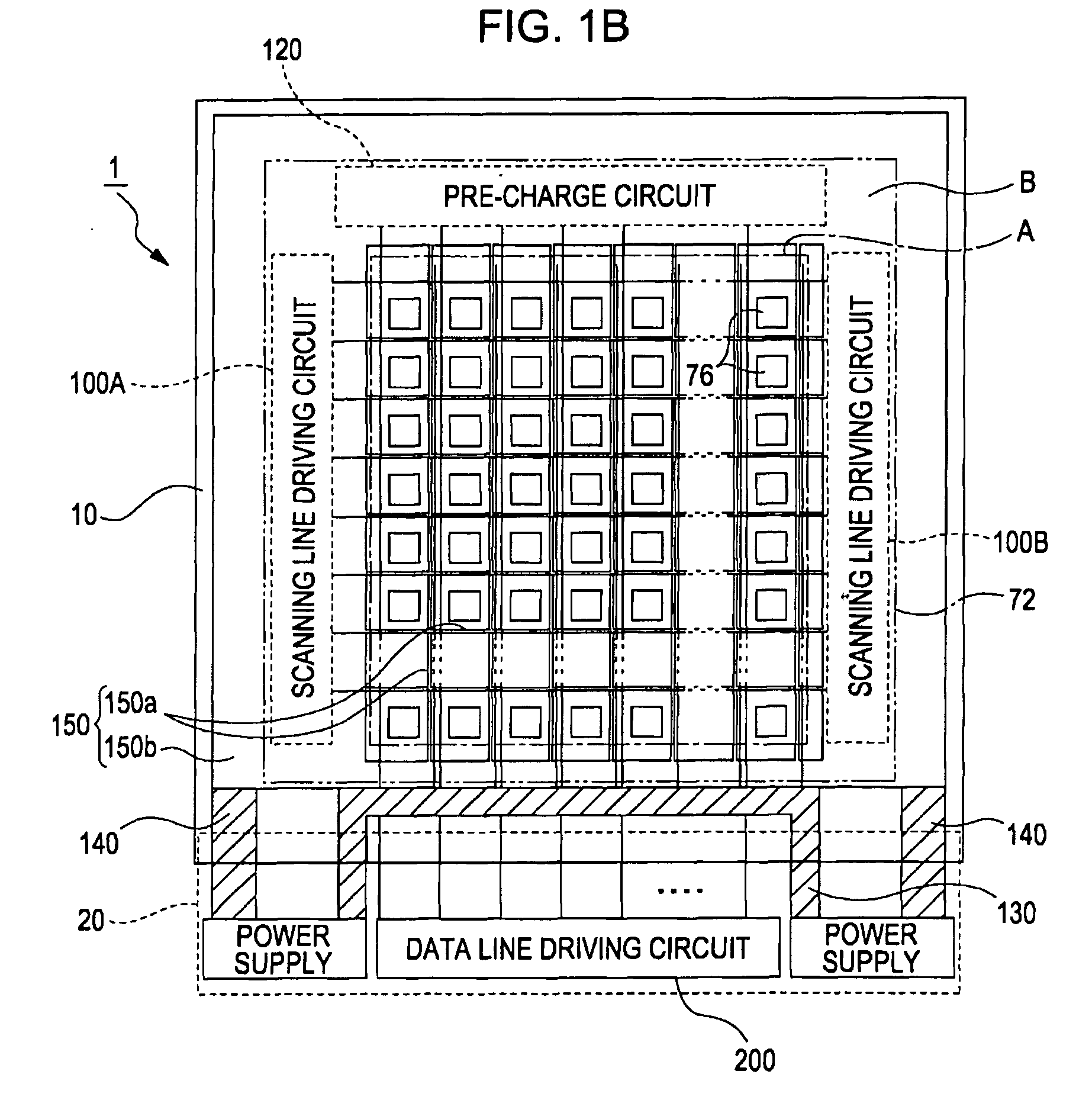
[0072]In the above described embodiment, the configuration in which the auxiliary electrode 150 and the pixel electrodes 76 are formed at the same time is described; however, the auxiliary electrode 150 may be formed not at the same time with the process of forming the pixel electrodes 76 but in the process after the partition wall 37 has been formed.

[0073]FIG. 7 is a partially cross-sectional view of a light emitting device 1A according to the present alternative embodiment. As shown in FIG. 7, in the light emitting device 1A, the auxiliary electrode 150 (150a, 150b) is formed to cover the second interlayer insulating film 35 and the partition wall 37. In the above described embodiment, as shown in FIG. 4, the auxiliary electrode 150 has a portion that is formed on the second interlayer insulating film 35 and the partition wall 37. In contrast, in this alternative embodiment, at a portion where the partition wall 37 is formed, the auxi...

second embodiment

B: Second Embodiment

[0077]Next, a light emitting device 1B according to a second embodiment of the invention will be described. The light emitting device 1B has the same configuration as the light emitting device 1, shown in FIG. 4, or the light emitting device 1A, shown in FIG. 7, according to the first embodiment except that the end portion E2 of the common electrode 72 is located on the outer side than the inner end portion E3 of the second electrode power supply line 140. Thus, the description thereof will be omitted where appropriate.

[0078]FIG. 8 is a partially schematic cross-sectional view of the light emitting device 1B. As shown in FIG. 8, in the light emitting device 1B, as in the case of the above described first embodiment, the end portion E2 of the common electrode 72 is formed on the outer side along the plane of the substrate 10 than the end portion E1 of the second interlayer insulating film 35 and formed on the inner side than the end portion E4 of the auxiliary ele...

third embodiment

C: Third Embodiment

[0080]Next, a light emitting device according to a third embodiment of the invention will be described. FIG. 9 is a partially cross-sectional view of a light emitting device 2A according to the present embodiment. As shown in FIG. 9, the auxiliary electrode 150 is formed on the common electrode 72 so as to be in plane contact, and the sealing film 80 is formed so as to cover the auxiliary electrode 150 and the common electrode 72. The light emitting device 2A has the same configuration as the light emitting device, shown in FIG. 7, according to the alternative embodiment to the first embodiment except that the common electrode 72 is formed in a lower layer under the auxiliary electrode 150. Thus, the description thereof will be omitted where appropriate.

[0081]As in the case of the above light emitting device 1A, in the present embodiment, the auxiliary electrode 150 is formed in an upper layer above the partition wall 37 at a portion where the partition wall 37 is...


PUM


Abstract

A light emitting device includes a substrate, a light emitting elements that have a first electrode, a second electrode and a light emitting layer, an element layer, an auxiliary electrode that is electrically connected to the second electrode, and an insulating layer. The second electrode is commonly provided for the light emitting elements. The insulating layer has a portion arranged in a lower layer under the second electrode and the auxiliary electrode. The auxiliary electrode is formed partly in a peripheral region of the light emitting device. In the peripheral region, an end portion of the second electrode is located on an inner side along a plane of the substrate than an end portion of the auxiliary electrode and located on an outer side than an end portion of the insulating layer.

Description

BACKGROUND[0001]1. Technical Field[0002]The present invention relates to a light emitting device that uses a light emitting element, such as an organic EL (electroluminescence) element.[0003]2. Related Art[0004]A light emitting device, in which a plurality of light emitting elements are arranged in an effective region on a substrate and various wirings, and the like, are arranged in a peripheral region that surrounds the effective region, has been known. Each of the light emitting elements includes a light emitting layer that is formed of a light emitting material, such as an organic EL material, and that is held between a first electrode and a second electrode. In most cases, the second electrode is a common electrode that is provided commonly for the plurality of light emitting elements and is provided all over the entire effective region. However, there is a possibility that a decrease in voltage will occur along the plane of the electrode because of a resistance of the electrode...

Claims


Application Information

Patent Timeline
IPC IPC(8): H01J29/96
CPCH01L27/3258H01L27/3276H01L27/3279H01L51/5228H01L51/5246H01L51/5203H10K59/124H10K59/1315H10K59/131H10K59/805H10K59/8722H10K59/80522H10K50/805H10K50/824H10K50/8426
Inventor KUBOTA, TAKEHIKO
Owner SEIKO EPSON CORP
Features
  • Generate Ideas
  • Intellectual Property
  • Life Sciences
  • Materials
  • Tech Scout
  • Unparalleled Data Quality
  • Higher Quality Content
  • 60% Fewer Hallucinations
Learn More