Dynamic sampling with efficient model for overlay

a dynamic sampling and efficient model technology, applied in semiconductor/solid-state device testing/measurement, instruments, total factory control, etc., can solve problems such as difficult optimization of sample plan for measuring overlay

Inactive Publication Date: 2008-08-21
INTEL CORP
View PDF3 Cites 33 Cited by
  • Summary
  • Abstract
  • Description
  • Claims
  • Application Information

AI Technical Summary

Problems solved by technology

However, as the wafer becomes larger and the design rules become tigh

Method used


Image

  • Dynamic sampling with efficient model for overlay
  • Dynamic sampling with efficient model for overlay
  • Dynamic sampling with efficient model for overlay

Examples


first embodiment

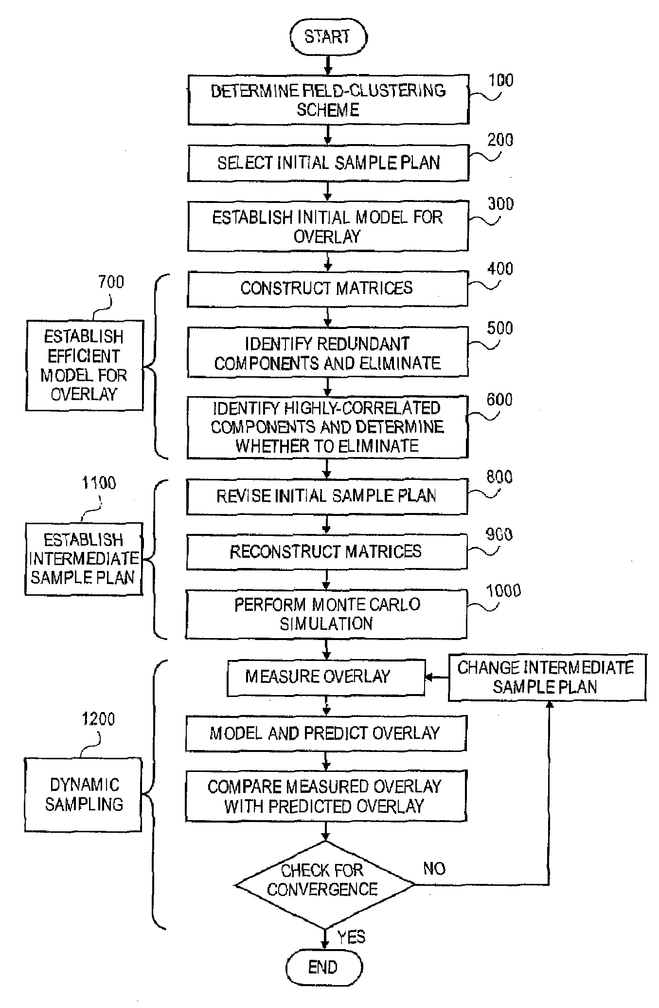
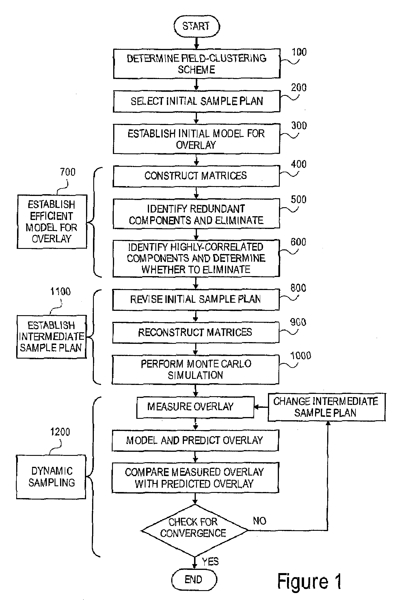
[0117]In the present invention, a single-point incremental algorithm may start with an empty or minimum-sized design, add one sampling site at a time to the sample plan, check for convergence, and continue iterating until the sample plan is optimized.

second embodiment

[0118]In the present invention, a multiple-point incremental algorithm may start with an empty or minimum-sized design, add certain multiple sampling sites at a time to the sample plan, check for convergence, and continue iterating until the sample plan is optimized.

third embodiment

[0119]In the present invention, a single-point decremental algorithm may start with a large or maximum-sized design, remove one sampling site at a time from the sample plan, check for convergence, and continue iterating until the sample plan is optimized.


PUM


Abstract

The present invention describes a method including: determining field-clustering scheme; selecting initial sample plan; establishing initial model of overlay, the initial model of overlay comprising components; and establishing efficient model of overlay from the initial model of overlay including: constructing matrices; identifying redundant components and eliminating the redundant components; and identifying highly-correlated components and determining whether to eliminate the highly-correlated components.

Description

CROSS-REFERENCE TO RELATED APPLICATION[0001]This application claims benefit of U.S. Patent Application Serial No. 10 / 956,608 filed on Sep. 30, 2004 and published as 20060074611 on Apr. 6, 2006.BACKGROUND OF THE INVENTION[0002]The present invention relates to the field of semiconductor integrated circuit manufacturing, and more specifically, to a method of optimizing a sample plan for measuring overlay.FIELD OF THE INVENTION[0003]The present invention relates to the field of semiconductor integrated circuit manufacturing, and more specifically, to a method of optimizing a sample plan for measuring overlay.DISCUSSION OF RELATED ART[0004]Integrated Circuit (IC) devices may be fabricated on a substrate, such as a wafer, that is usually made from semiconducting material, such as silicon. Various types of materials may be added to, or removed from, the wafer during processing. The materials may include insulating material, such as silicon oxide, or conducting material, such as copper.[000...

Claims


Application Information

Patent Timeline
IPC IPC(8): G06F17/50
CPCG06F17/5009H01L22/20G06F2217/12G06F2217/10G06F30/20G06F2111/08G06F2119/18Y02P90/02
Inventor WONG, ALANDRAUTZ, JEFFSHINDLER, JOSEPH D.LAU, MAXCHEN, GEORGE
Owner INTEL CORP
Why Eureka
Try Eureka