Semiconductor device and method for reducing power consumption in a system having interconnected devices

Inactive Publication Date: 2008-08-21
CONVERSANT INTPROP MANAGEMENT INC
View PDF99 Cites 52 Cited by
  • Summary
  • Abstract
  • Description
  • Claims
  • Application Information

AI Technical Summary

Benefits of technology

[0012]A memory device according to another embodiment of the present invention does not forward the input command to the next memory device when there is an ID match. Therefore, the memory devices that do not receive the command will not perform operations at the normal power consumption level, with the result that the power consumption by the system will be red

Problems solved by technology

However, this approach does not guarantee good signal integrity and enough t

Method used


Image

  • Semiconductor device and method for reducing power consumption in a system having interconnected devices
  • Semiconductor device and method for reducing power consumption in a system having interconnected devices
  • Semiconductor device and method for reducing power consumption in a system having interconnected devices

Examples


Example

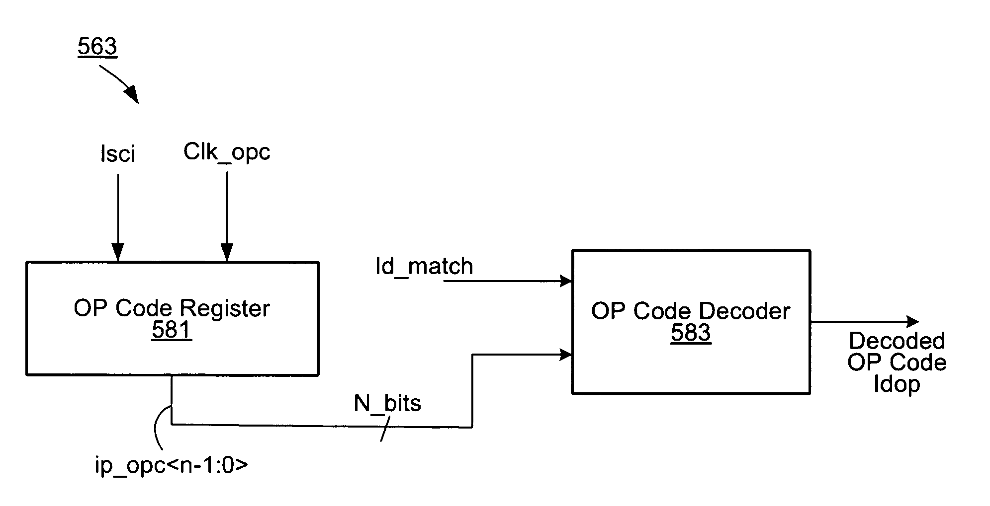
[0033]In the following detailed description of sample embodiments of the invention, reference is made to the accompanying drawings which form a part hereof, and in which is shown by way of illustration specific sample embodiments in which the present invention may be practiced. These embodiments are described in sufficient detail to enable those skilled in the art to practice the present invention, and it is to be understood that other embodiments may be utilized and that logical, mechanical, electrical, and other changes may be made without departing from the scope of the present invention. The following detailed description is, therefore, not to be taken in a limiting sense, and the scope of the present invention is defined by the appended claims.

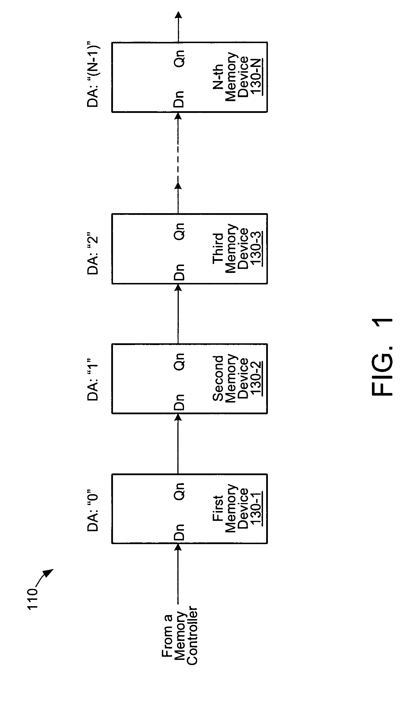
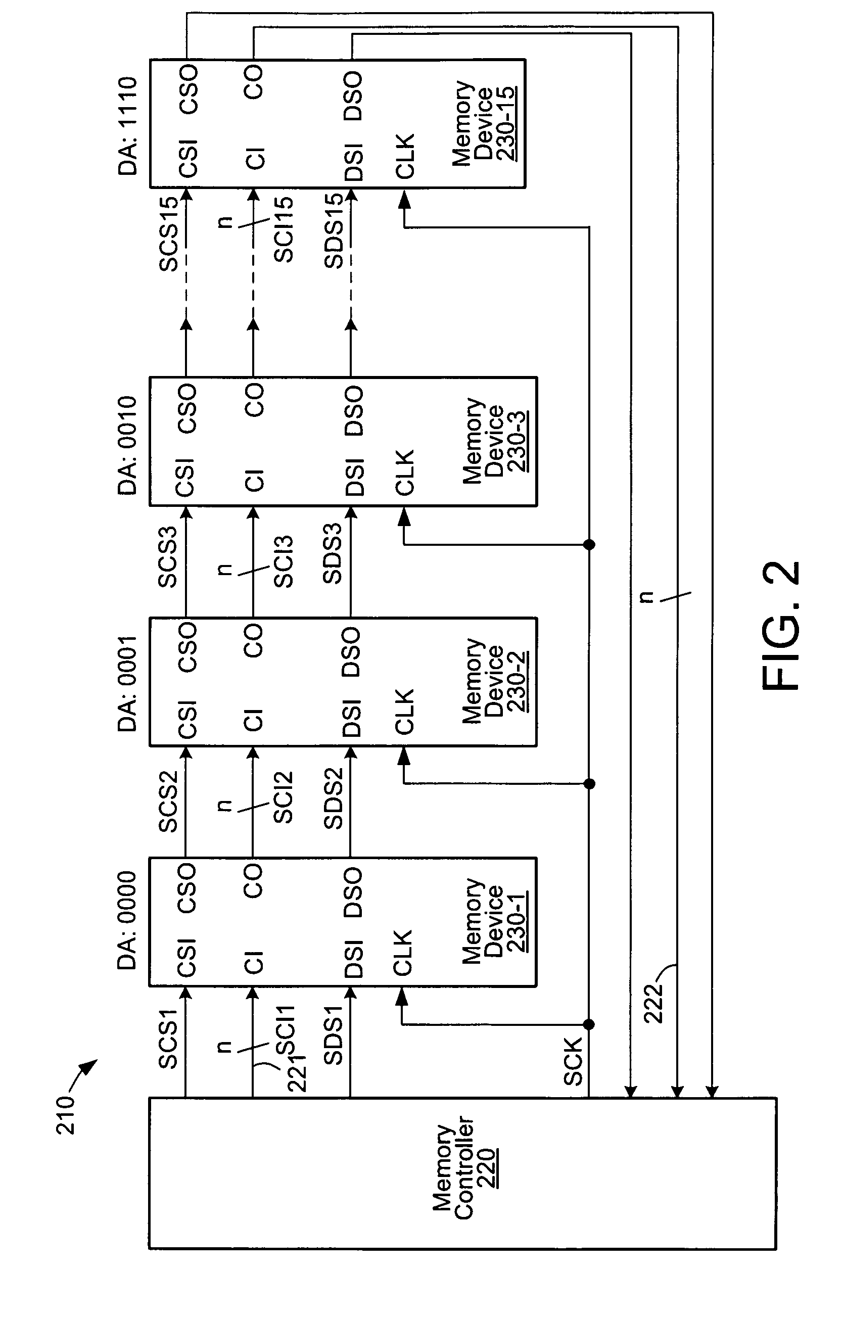
[0034]The present invention relates generally to a system having an arrangement including a plurality of semiconductor devices. The devices may operate with different power consumption levels. Examples of the semiconductor devices are pro...


PUM


Abstract

A system includes a plurality of memory devices connected in-series that communicate with a memory controller. A memory device designated by an ID number performs operations at a normal power consumption level. The other devices not designated perform signal forwarding operations at a reduced power consumption level. The designated memory device enables its internal clock generator to generate all clocks necessary for operations. The non-designated memory devices generate clocks to perform partial operations for forwarding commands to next memory devices. In another example, memory devices do not forward the input command to the next memory device when there is no ID match. In another example, a memory device transmits the command replacing the content thereof with a static output when there is an ID match. Such partial clock generation, non-forwarding of commands and replacing the command contents will cause the system to operate at the reduced power consumption level.

Description

CROSS REFERENCE TO RELATED APPLICATIONS[0001]This application claims the benefit of priority from U.S. Provisional Patent Application No. 60 / 902,003 filed Feb. 16, 2007; U.S. Provisional Patent Application No. 60 / 891,108 filed Feb. 22, 2007; and U.S. Provisional Patent Application No. 60 / 943,442 filed Jun. 12, 2007, the he disclosures of which are expressly incorporated herein by reference in their entirety.FIELD OF THE INVENTION[0002]The present invention relates generally to semiconductor devices. More particularly, the present invention relates to a system having an arrangement having a plurality of semiconductor devices.BACKGROUND OF THE INVENTION[0003]Power consumption control is important in memory and system design, and there are potential benefits in reducing power consumption. For instance, a memory system that is battery-powered benefits from a longer battery life if power consumption by the memory system is reduced. There also are benefits in reducing power consumption fo...

Claims


Application Information

Patent Timeline
IPC IPC(8): G06F1/32
CPCG11C19/00G11C5/14G11C7/22G11C8/12G11C8/18
Inventor PYEON, HONG BEOMKIM, JIN-KIOH, HAKJUNE
Owner CONVERSANT INTPROP MANAGEMENT INC
Why Eureka
Try Eureka