Method for Preparing an Electric Circuit Comprising Multiple Leds

a technology of leds and circuits, applied in the field of electric circuits, can solve the problems of time-consuming and labor-intensive bridge circuits, long connections between components, and complex connections between components, so as to improve the production efficiency of electric components in circuits and reduce the length of connections

Inactive Publication Date: 2008-08-28
LEMNIS LIGHTING PATENT HLDG
View PDF5 Cites 49 Cited by
  • Summary
  • Abstract
  • Description
  • Claims
  • Application Information

AI Technical Summary

Benefits of technology

[0002]The invention aims at realizing a more efficient circuit in which the length of the connections can be reduced and also the production efficiency of the electric components in a circuit can be improved. This aim is achieved by providing a method for preparing an electric circuit comprising a plurality of LEDs, which comprises the following steps:

Problems solved by technology

The manufacture of such a bridge circuit with a number of diode components, such as Light-Emitting Diodes (LEDs) in chips is time-consuming because the chips must be placed by a placing apparatus in the proper orientation, which differs for the respective diodes, while in the current methods they are supplied in the same orientation.
Connecting all components is also complex.
This complexity leads to long connections between components.
Due to the long connections additional energy losses occur and unnecessary heat is generated.

Method used


Image

  • Method for Preparing an Electric Circuit Comprising Multiple Leds
  • Method for Preparing an Electric Circuit Comprising Multiple Leds
  • Method for Preparing an Electric Circuit Comprising Multiple Leds

Examples


first embodiment

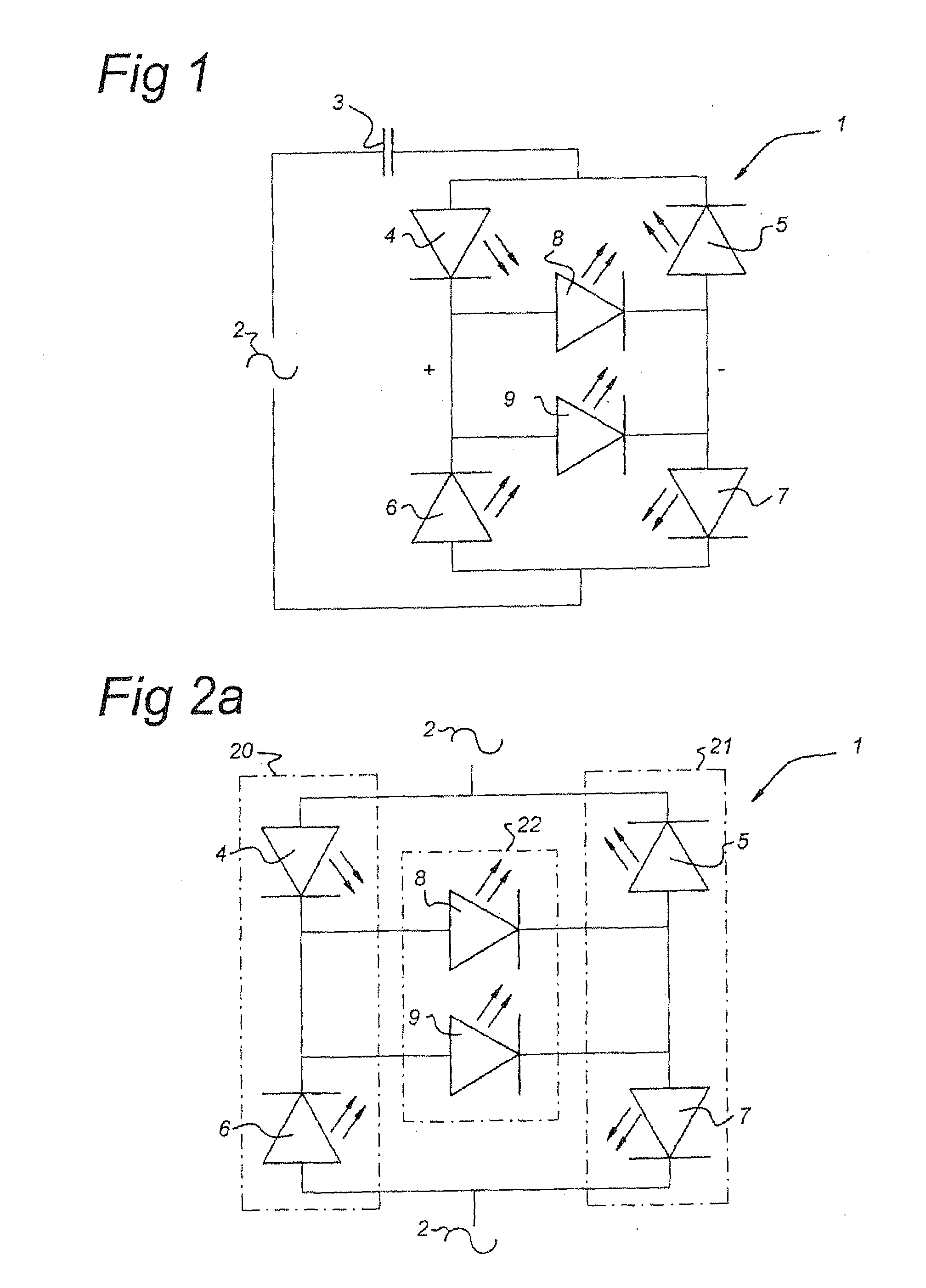
[0025]In a first embodiment the invention relates to a method comprising the following steps:[0026]providing a first substrate comprising an emitting side and an attachment side, in which the first substrate comprises a first layer of a first semiconductor type and a second layer of a semiconductor type according to a first pattern, in which the second layer is disposed on the attachment side of the first substrate;[0027]attaching the attachment side of the first substrate to the second substrate, the second substrate being insulating and provided with a second pattern of at least one conducting layer; and[0028]cutting the first substrate from the emitting side of the first substrate down to the second pattern of the at least one conducting layer according to a third pattern, forming the plurality of LEDs.

[0029]Because the second pattern of the at least one conducting layer on the second substrate provides for the forming of connections between the LEDs, the LEDs need not be placed ...

second embodiment

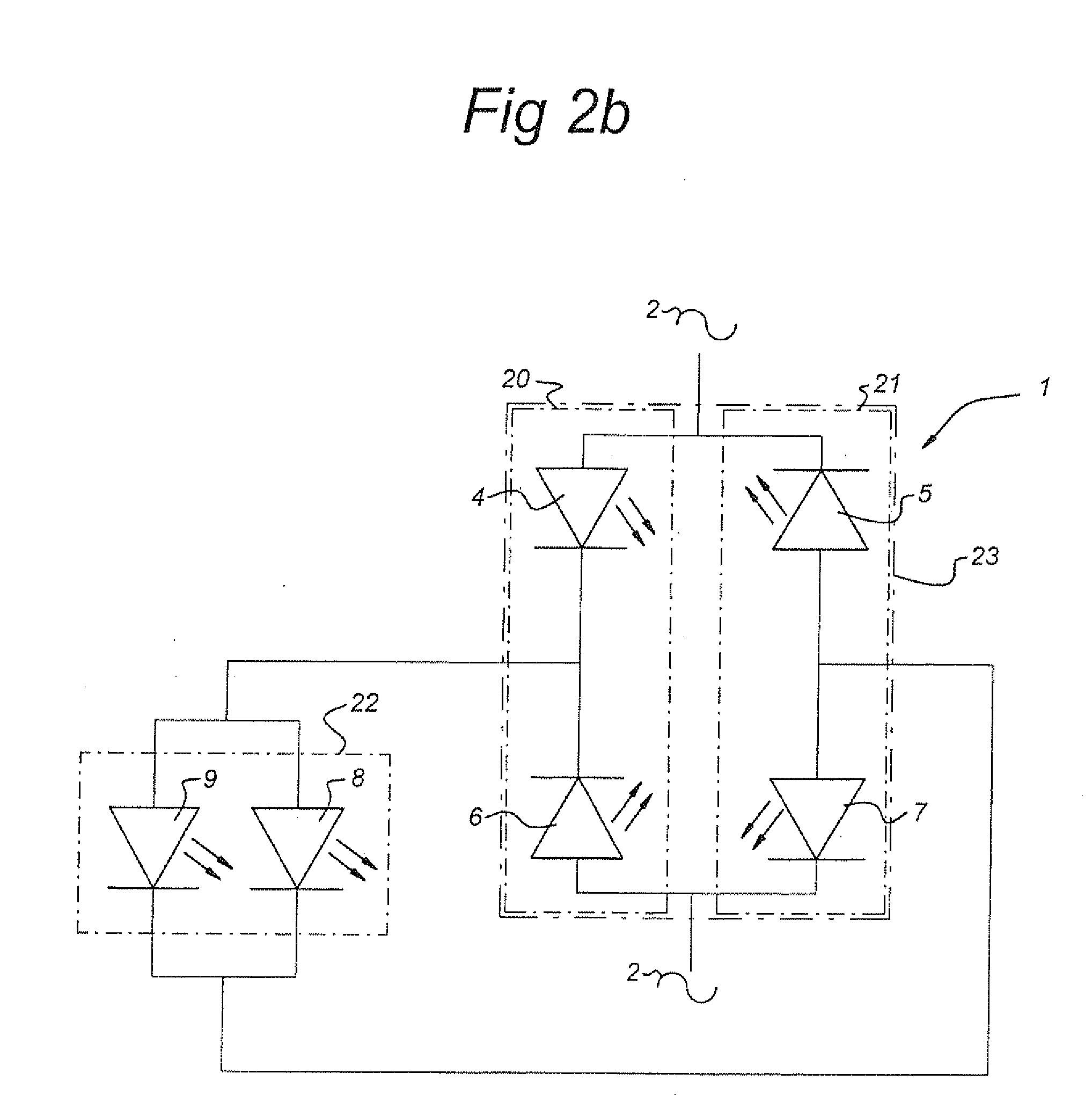
[0035]In a second embodiment the invention relates to a method for preparing an electric circuit comprising a plurality of LEDs, in which the method comprises the following steps:[0036]providing a first insulating substrate transparent for a wavelength that can be generated by at least one of the plurality of LEDs;[0037]forming a layer on the first insulating substrate, comprising a first layer of a first semiconductor type, and a second layer of a second semiconductor type;[0038]selectively removing the second layer according to a first pattern, until part of the first layer is exposed, and at least by grooves an isolated area of the second semiconductor type is formed;[0039]selectively applying at least one conducting layer according to a second pattern, thereby making a first connection with the first layer of the first semiconductor type and a second connection with the isolated area of the second semiconductor type;[0040]cutting through the at least one conducting layer, the se...


PUM


Abstract

The invention relates to a method for preparing an electric circuit comprising a plurality of Light-Emitting Diodes (LEDs). First, a continuous layer of a first semiconductor material is provided. On this a first pattern of a material of a second semiconductor type is applied. Next, a substrate comprising a second pattern of at least one conducting layer (34) is attached to the first pattern. After this, the continuous layer is cut according to a third pattern. Thus the plurality of LEDs is formed.

Description

BACKGROUND OF THE INVENTION[0001]The present invention relates to an electric circuit comprising at least one semiconductor component. A circuit for which the present invention is suitable is described in Dutch application NL1027960. In this application, which is incorporated herein by reference in its entirety, a bridge circuit is described, among others, having such a set up that at least four rectifiers, preferably diodes, supply a rectified current to at least one lighting element. The manufacture of such a bridge circuit with a number of diode components, such as Light-Emitting Diodes (LEDs) in chips is time-consuming because the chips must be placed by a placing apparatus in the proper orientation, which differs for the respective diodes, while in the current methods they are supplied in the same orientation. Connecting all components is also complex. This complexity leads to long connections between components. Due to the long connections additional energy losses occur and un...

Claims


Application Information

Patent Timeline
Patent Type & Authority Applications(United States)
IPC IPC(8): H01L33/00H01L21/00H05B44/00
CPCH01L25/0753H01L33/0079H01L33/0095H01L2924/3011H05B33/0821H01L2924/0002H05B33/0857H01L2924/00H05B45/40H05B45/20H01L33/0093
Inventor ROOYMANS, JOHANNES OTTO
Owner LEMNIS LIGHTING PATENT HLDG
Why Eureka
Try Eureka