Liquid crystal device

a liquid crystal device and liquid crystal technology, applied in non-linear optics, instruments, optics, etc., can solve the problems of inability to maintain a sufficient amount of display light, the quality of the display image may be easily degraded, and the disadvantage of the va mode liquid crystal device, etc., to achieve the effect of high-quality imag

Active Publication Date: 2008-08-28
JAPAN DISPLAY WEST
View PDF7 Cites 12 Cited by
  • Summary
  • Abstract
  • Description
  • Claims
  • Application Information

AI Technical Summary

Benefits of technology

[0007]An advantage of some aspects of the invention is to provide a liquid crystal device capable of displaying a high-quality image even when a storage capacitor is formed with a capacitor line of a desired width.
[0008]In addition, another advantage of some aspects of the invention is to provide a liquid crystal device capable of reducing a resistance of the capacitor line when the capacitor line is formed with the capacitor line of a desired width.
[0010]According to the first aspect of the invention, in the case of providing such a storage capacitor constituted by the capacitor line, the capacitor line includes the first capacitor line portion, and the second capacitor line portion. The first capacitor line portion is at the position close to the scanning line and extends in parallel with the scanning line. The second capacitor line portion is formed so as to overlap the cutouts provided between the sub-pixel electrodes. The storage capacitor includes the first storage capacitor and the second storage capacitor. Therefore, even when the first capacitor line portion is not formed so as to have a large width, a storage capacitor having a sufficient capacitance can be formed. Since the second capacitor line portion is formed so as to overlap a domain region which does not contribute to display, an amount of emitted display light does not decrease even when the second capacitor line portion is added, and thereby a high quality image can be displayed.
[0012]According to the second aspect of the invention, in a VA mode liquid crystal device in the case of providing such a storage capacitor constituted by the capacitor line, the capacitor line includes the first capacitor line portion, and the second capacitor line portion. The first capacitor line portion is at the position close to the scanning line and extends in parallel with the scanning line. The second capacitor line portion is formed so as to overlap the region provided between the sub-pixel electrodes. The storage capacitor includes the first storage capacitor and the second storage capacitor. Therefore, even though the first capacitor line portion is not formed so as to have a large width, a storage capacitor having a sufficient capacitance can be formed. Since the second capacitor line portion is formed so as to overlap the region provided between the sub-pixel electrodes which does not contribute to display, an amount of emitted display light does not decrease even when the second capacitor line portion is added, and thereby a high quality image can be displayed.
[0014]According to the third aspect of the invention, in an IPS mode liquid crystal device in the case of providing such a storage capacitor constituted by the capacitor line, the capacitor line includes the first capacitor line portion which extends in parallel with the corresponding one of the scanning lines at the position close to the scanning line and the second capacitor line portion that is formed so as to overlap the bent portions of the pectinate-shaped electrodes. The storage capacitor can be formed, constituted by the first and the second capacitor line portions. Therefore, a storage capacitor having a sufficient capacitance can be formed even though the first capacitor line portion is not formed so as to have a large width. In addition, the second capacitor line portion is formed so as to overlap the bent portions of the pectinate-shaped electrodes. Such an overlapping region does not contribute to display. Therefore, since an amount of emitted display light does not decrease even when the second capacitor line portion is added, and thereby a high quality image can be displayed.
[0016]According to the first aspect of the invention, it is preferable that each of the capacitor lines may further include a third capacitor line portion which extends so as to overlap a corresponding one of the data lines and connects the first capacitor line portion and the second capacitor line portion. Such a structure does not decrease an aperture ratio per pixel even when the third capacitor line portion is added since the third capacitor line portion extends so as to overlap the corresponding one of the data lines. In addition, if a third storage capacitor is also formed at the third capacitor line portion, the storage capacitor having a sufficient capacity can be formed even in the case where the first and the second capacitor line portions are formed to have a small width.

Problems solved by technology

Therefore, in such a VA mode liquid crystal device, providing a sufficient capacitance to the storage capacitor 60 leads to a disadvantage that the quality of a display image may be easily degraded; for example, sufficient amount of display light may not be able to be maintained.
Such a disadvantage exists not only for the VA mode liquid crystal device but also for, for example, an IPS (in-plane switching) mode liquid crystal device, in which a liquid crystal is driven by a horizontal electric field.
Thus, in the IPS mode liquid crystal device, forming a storage capacitor having a sufficient capacitance also leads to a disadvantage that the quality of a display image may be easily degraded; for example, a sufficient amount of display light may not be able to be maintained.

Method used


Image

  • Liquid crystal device
  • Liquid crystal device
  • Liquid crystal device

Examples


first embodiment

Advantage(s) of First Embodiment

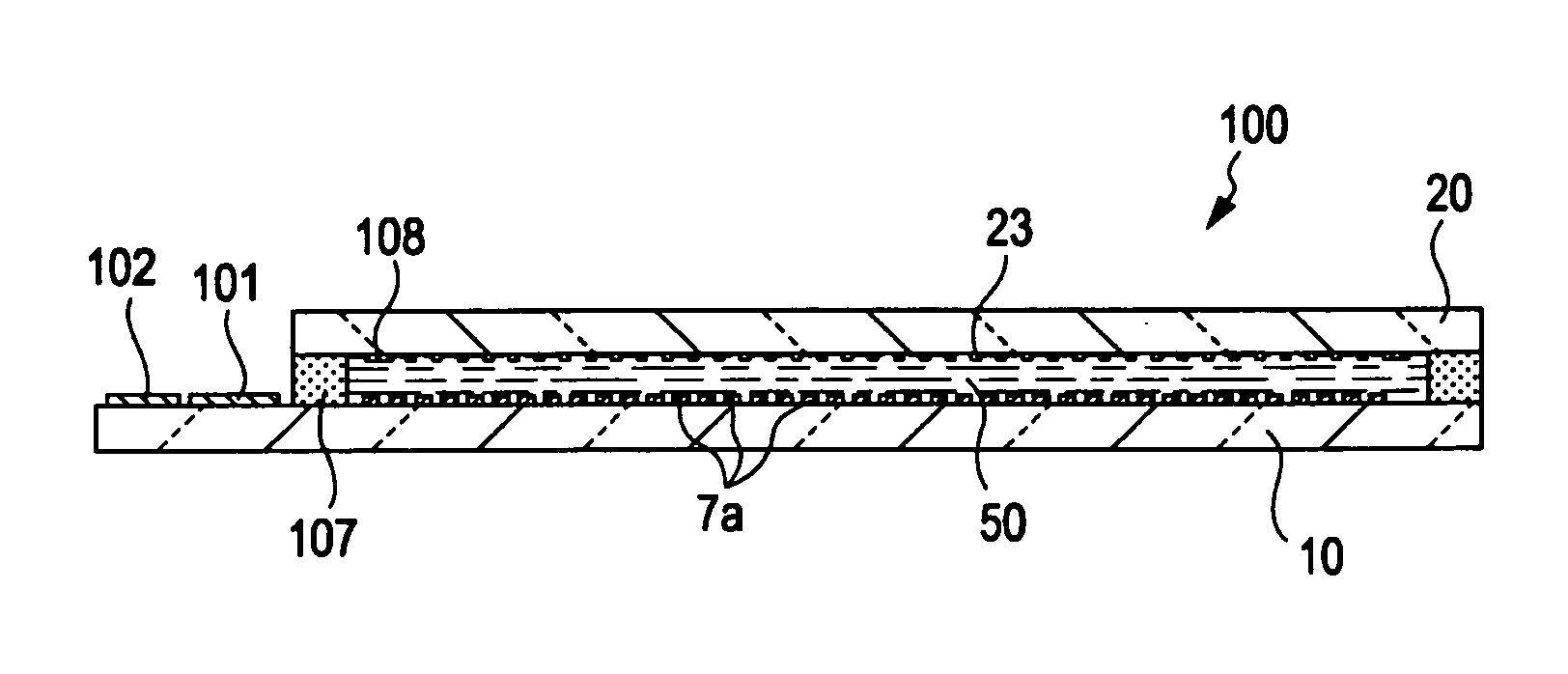
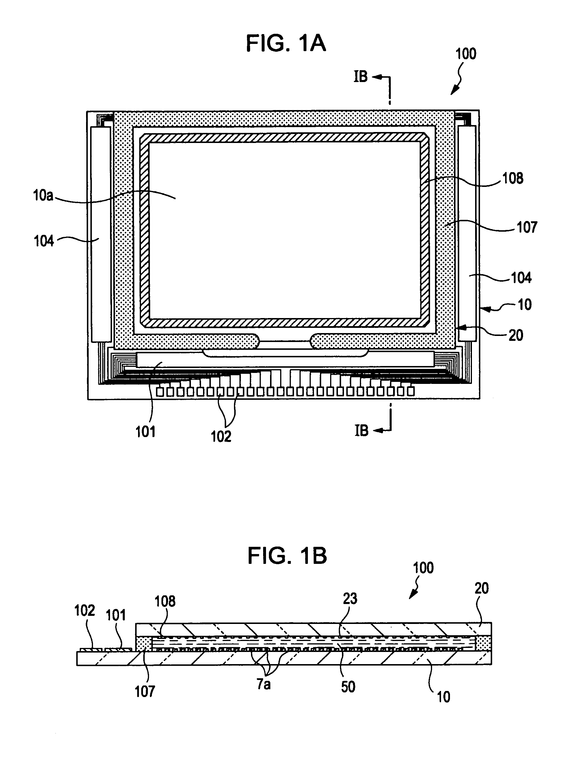
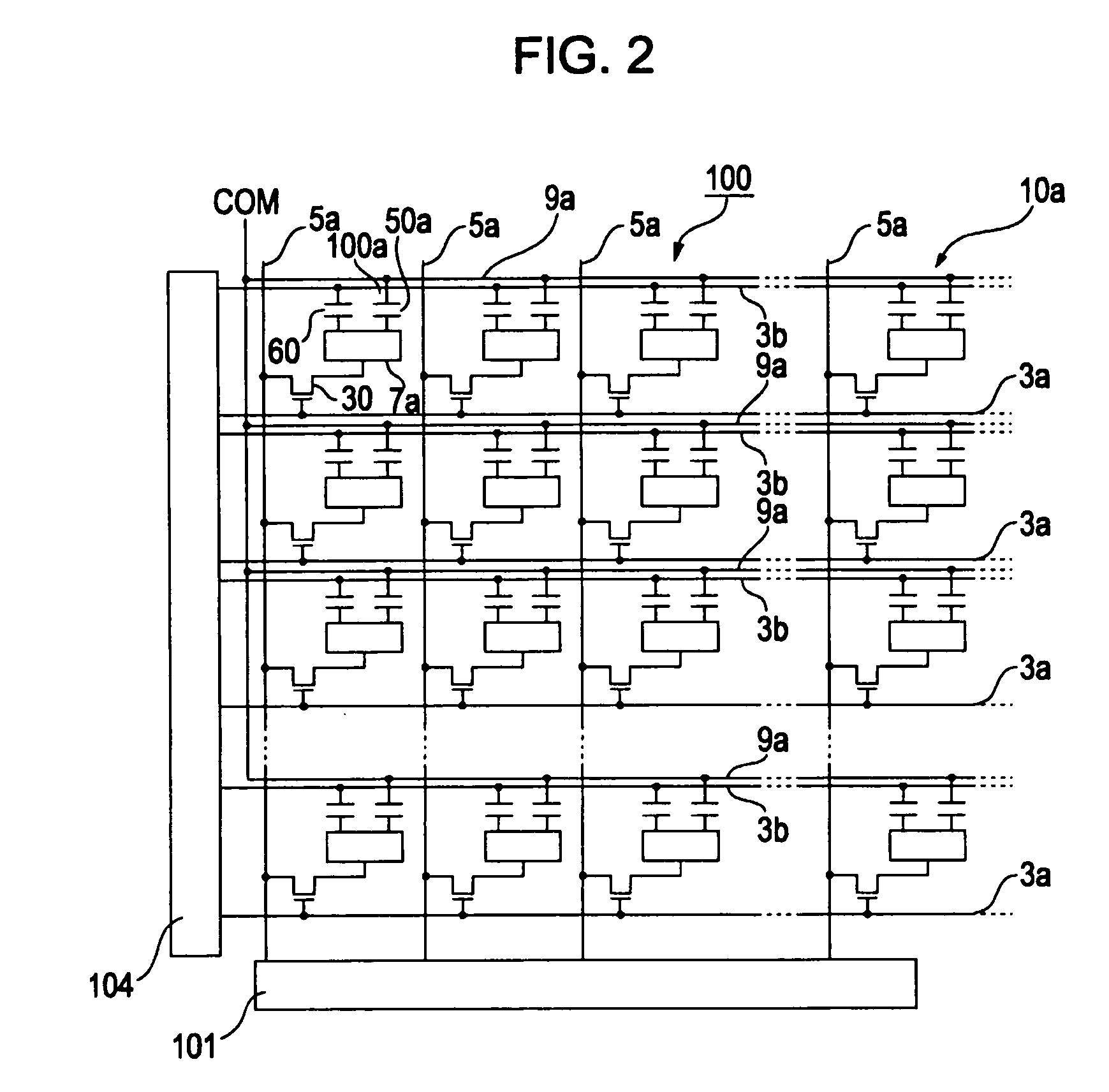
[0051]As described above, the capacitor line 3b includes the first capacitor line portion 3c, the second capacitor line portion 3d, and the third capacitor line portion 3e in the liquid crystal device 100 of the first embodiment, the liquid crystal device 100 being driven in the VA mode. The first capacitor line portion 3c is at the position close to the corresponding one of the scanning lines 3a and extends in parallel with the scanning line 3a. The second capacitor line portion 3d is formed so as to overlap the cutouts 7f provided between the sub-pixel electrodes 7b and 7c. The third capacitor line portion 3e connects the first capacitor line portion 3c to the second capacitor line portion 3d. The storage capacitor 60 includes the first storage capacitor 60a, the second storage capacitor 60b, and the third storage capacitor 60c, which are formed by utilizing the capacitor line portions 3c, 3d, and 3e, respectively. Here, the first capacitor line por...

second embodiment

Advantage(s) of Second Embodiment

[0067]As described above, the capacitor line 3b includes the first capacitor line portion 3c, the second capacitor line portion 3d, and the third capacitor line portion 3e in the liquid crystal device 100 of the second embodiment, the liquid crystal device 100 being driven in the IPS mode. The first capacitor line portion 3c is at the position close to the corresponding one of the scanning lines 3a and extends in parallel with the scanning line 3a. The second capacitor line portion 3d is formed so as to overlap the bent portions 7i of the pixel electrode 7a and the bent portions 9i of the common electrode 9a. The third capacitor line portion 3e connects the first capacitor line portion 3c and the second capacitor line portion 3d. The first storage capacitor 60a, the second storage capacitor 60b, and the third storage capacitor 60c are formed by utilizing the first capacitor line portion 3c, the second capacitor line portion 3d, and the third capacito...


PUM

PropertyMeasurementUnit
thicknessaaaaaaaaaa
dielectric constantaaaaaaaaaa
heightaaaaaaaaaa

Abstract

A liquid crystal device have an element substrate including a scanning line, a data line and a pixel electrode, a cutout is formed on the pixel electrode. A capacitor line for providing a storage capacitor is formed on the element substrate. The capacitor line has a first and second portions. The first portion extends along with the scanning line, and a second line portion overlaps the cutout of the pixel electrode.

Description

BACKGROUND[0001]1. Technical Field[0002]The present invention relates to a liquid crystal device having a plurality of pixels that each have a pixel switching element, a pixel electrode, and a storage capacitor. More particularly, the invention relates to a structure of a capacitor line for providing a storage capacitor.[0003]2. Related Art[0004]A typical technique for improving viewing angle characteristics of a liquid crystal device may be used to produce a vertical alignment (VA) mode liquid crystal device. A VA mode liquid crystal device uses a nematic liquid crystal material having a negative anisotropy of dielectric constant as a liquid crystal material and a vertical alignment film. For such a liquid crystal device, dividing a pixel electrode into a plurality of sub-pixel electrodes connected with a connecting portion therebetween in order to control an alignment of a liquid crystal has been proposed (See JP-A-2003-228073).[0005]In such a VA mode liquid crystal device, when a...

Claims


Application Information

Patent Timeline
Patent Type & Authority Applications(United States)
IPC IPC(8): G02F1/1343
CPCG02F1/136213G02F2201/40G02F1/1393G02F1/1343
Inventor FUJITA, SHIN
Owner JAPAN DISPLAY WEST
Why Eureka
Try Eureka