
Method for fabricating strained-silicon metal-oxide semiconductor transistors

Active Publication Date: 2008-08-28
MARLIN SEMICON LTD
View PDF5 Cites 6 Cited by
  • Summary
  • Abstract
  • Description
  • Claims
  • Application Information

AI Technical Summary

Benefits of technology

[0014]According to the preferred embodiment of the present invention, a second rapid thermal annealing process is specifically conducted after the formation of the epitaxial layer to improve the deactivation phenomenon caused by the baking process. It should be noted that this second rapid thermal annealing process not only redefines the distribution of dopants within the semiconductor substrate, but also repairs the bonds that are damaged by the lowered temperature of the baking process, thus increasing the overall performance of the MOS transistor.

Problems solved by technology

However, it has been recently pointed out that the miniaturization attained by a lithographic technology has reached its limit.
This step provides a growing surface for the epitaxial layer but also causes the dopants within the source / drain region to be gathered in the edge region of the recess, thereby inducing an uneven distribution of dopants and affecting the performance of the MOS transistor.
Secondly, after the formation of the source / drain region, a rapid thermal annealing process is conducted to activate the injected dopants by diffusing the dopants throughout the source / drain region.
Despite the fact that the baking process provides an ideal growing surface for the epitaxial layer, this lowered temperature carried by the baking process would disrupt the bonding of the dopants, which ultimately increases the overall resistance and induces a deactivation phenomenon.
As discussed previously, an increase in resistance would result in a deactivation phenomenon and damage the bonds within the dopants.

Method used


Image

  • Method for fabricating strained-silicon metal-oxide semiconductor transistors
  • Method for fabricating strained-silicon metal-oxide semiconductor transistors
  • Method for fabricating strained-silicon metal-oxide semiconductor transistors

Examples


Embodiment Construction

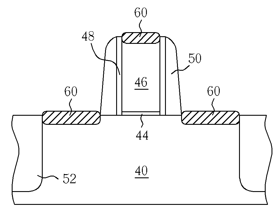
[0021]Please refer to FIGS. 7-10. FIGS. 7-10 illustrate a method of utilizing selective epitaxial growth process for fabricating a strained-silicon metal-oxide semiconductor transistor according to the preferred embodiment of the present invention. As shown in FIG. 7, a semiconductor substrate 40, such as a silicon substrate is first provided. The semiconductor substrate 40 includes a gate structure 42 thereon, in which the gate structure 42 includes a gate dielectric 44 and a gate 46 disposed on the gate dielectric 44. An ion implantation process is performed thereafter to inject a p-type or n-type dopant of smaller concentration into the semiconductor substrate 40. The implantation process preferably forms a lightly doped drain 54 in the semiconductor substrate 40 surrounding the gate structure 42. An offset spacer 48 is formed on the sidewall of the gate structure 42 and a spacer 50 is formed around the offset spacer 48 thereafter. Preferably, the gate dielectric 44 is composed i...


PUM


Abstract

A method for fabricating strained-silicon transistors is disclosed. First, a semiconductor substrate is provided and a gate structure and a spacer surrounding the gate structure are disposed on the semiconductor substrate. A source / drain region is then formed in the semiconductor substrate around the spacer, and a first rapid thermal annealing process is performed to activate the dopants within the source / drain region. An etching process is performed to form a recess around the gate structure and a selective epitaxial growth process is performed to form an epitaxial layer in the recess. A second rapid thermal annealing process is performed to redefine the distribution of the dopants within the source / drain region and repair the damaged bonds of the dopants.

Description

BACKGROUND OF THE INVENTION[0001]1. Field of the Invention[0002]The invention relates to a method for fabricating strained-silicon transistors.[0003]2. Description of the Prior Art[0004]The performance of MOS transistors has increased year after year with the diminution of critical dimensions and the advance of large-scale integrated circuits (LSI). However, it has been recently pointed out that the miniaturization attained by a lithographic technology has reached its limit. Therefore, how to improve the carrier mobility so as to increase the speed performance of MOS transistors has become a major topic for study in the semiconductor field. For the known arts, attempts have been made to use a strained silicon layer, which has been grown epitaxially on a silicon substrate with a silicon germanium (SiGe) layer disposed therebetween. In this type of MOS transistor, a biaxial tensile strain occurs in the epitaxy silicon layer due to the silicon germanium which has a larger lattice const...

Claims


Application Information

Patent Timeline
IPC IPC(8): H01L21/8238H01L21/336
CPCH01L21/823807H01L21/823814H01L29/165H01L29/7848H01L29/6656H01L29/66628H01L29/66636H01L29/66545
Inventor TING, SHYH-FANNHUANG, CHENG-TUNGJENG, LI-SHIANLEE, KUN-HSIENHUNG, WEN-HANCHENG, TZYY-MINGWU, MENG-YIHSIAO, TSAI-FUCHAN, SHU-YEN
Owner MARLIN SEMICON LTD
Features
  • Generate Ideas
  • Intellectual Property
  • Life Sciences
  • Materials
  • Tech Scout
  • Unparalleled Data Quality
  • Higher Quality Content
  • 60% Fewer Hallucinations
Learn More